4 in-circuit debug flag, 5 in-circuit debug buff, 4 in-circuit debug flag register (icdf) -7 – Maxim Integrated MAXQ7667 User Manual
Page 205: 5 in-circuit debug buffer register (icdb) -7, Maxq7667 user’s guide, 4 in-circuit debug flag register (icdf), 5 in-circuit debug buffer register (icdb)

12-7
__________________________________________________________________________________________________________
MAXQ7667 User’s Guide
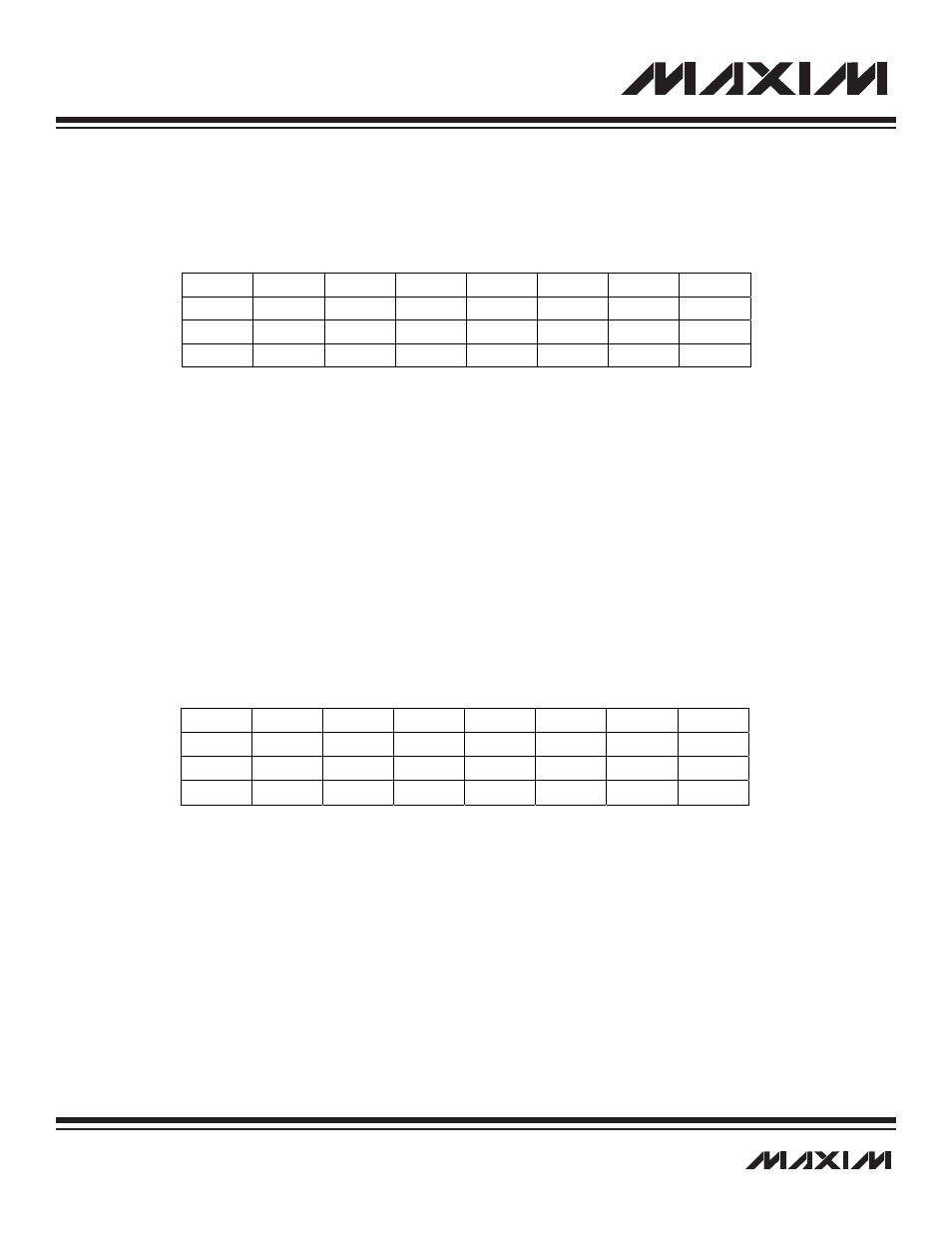
12.2.4 In-Circuit Debug Flag Register (ICDF)
Register Description:
In-Circuit Debug Flag Register
Register Name:
ICDF
Register Address:
Module 02h, Index 1Bh
Bits 7 to 4: Reserved. Read 0, write ignored.
Bits 3 and 2: Programming Source Select Bits 1 and 0 (PSS[1:0]). See Section 13 for information on these bits.
Bit 1: System Program Enable (SPE). See Section 13 for information on this bit.
Bit 0: Serial Transfer Enable (TXC). This bit is set by hardware at the end of a transfer cycle at the TAP communication link. The TXC
bit helps the debug engine to recognize host requests, either command or data. This bit is normally set by ROM code to signify or
request the sending or receiving of data. Once set, the debug engine clears the TXC bit. CPU writes to the TXC bit result in the clear-
ing of the JTAG PSS[1:0] bits.
12.2.5 In-Circuit Debug Buffer Register (ICDB)
The ICDB register serves as the parallel holding buffer for the debug shift register of the TAP. Data is read from or written to ICDB for
serial communication between the debug routines and the external host. This register is cleared to 00h after a power-on reset or a test-
logic-reset TAP state.
Register Description:
In-Circuit Debug Buffer Register
Register Name:
ICDB
Register Address:
Module 02, Index 1Ch
Bits 7 to 0: In-Circuit Debug Buffer Register Bits 7:0 (ICDB[7:0])
Bit #
7
6
5
4
3
2
1
0
Name
—
—
—
—
PSS1
PSS0
SPE
TXC
Reset
0
0
0
0
0
0
0
0
Access
r
r
r
r
rw
rw
rw
rw
r = read, w = write
Bit #
7
6
5
4
3
2
1
0
Name
ICDB7
ICDB6
ICDB5
ICDB4
ICDB3
ICDB2
ICDB1
ICDB0
Reset
0
0
0
0
0
0
0
0
Access
rw
rw
rw
rw
rw
rw
rw
rw
r = read, w = write
