6 system control registe, 6 system control register (sc) -9, Maxq7667 user’s guide – Maxim Integrated MAXQ7667 User Manual
Page 53: 6 system control register (sc)
4-9
___________________________________________________________________________________________________________
MAXQ7667 User’s Guide
4.1.6 System Control Register (SC)
Register Description:
System Control Register
Register Name:
SC
Register Address:
Module 08h, Index 08h
Bit 7: Test Access (JTAG) Port Enable (TAP). This bit controls whether the Test Access Port special-function pins are enabled. The
TAP defaults to being enabled. Clearing this bit to 0 disables the TAP special function pins. See Section 11 for more information about
JTAG and TAP.
Bits 6 and 0: Reserved. Read 0, write ignored.
Bits 5 and 4: Code Data Access Bits 1 and 0 (CDA[1:0]). The CDA bits are used to logically map physical program memory page
to the data space for read/write access (see table below).
The logical data memory addresses of the program pages depend on whether execution is from Utility ROM or logical data memory.
Note that CDA1 is not implemented if the upper 32k of the program space is not used for the user code. No CDA bits are needed if
only one page of program space is incorporated. (P0 is the only memory available in the MAXQ7667.)
Bit 3: Upper Program Access (UPA). The physical program memory is logically divided into four pages; P0 and P1 occupy the lower
32KWords while P2 and P3 occupy the upper 32KWords. P0 and P1 are assigned to the lower half of the program space and are always
active. P2 and P3 must be explicitly activated in the upper half of the program space by setting the UPA bit to 1. When UPA bit is
cleared to 0, the upper program memory space is occupied by the utility ROM and the logical data memory, which is accessible as
program memory. Note that the UPA is not implemented if the upper 32K of the program space is not used for the user code.
Bit 2: ROM Operation Done (ROD). This bit is used to signify completion of a ROM operation sequence to the control units. This allows
the debug engine to determine the status of a ROM sequence. Setting this bit to logic 1 causes an internal system reset if the JTAG
SPE bit is also set. Setting the ROD bit will clear the JTAG SPE bit if it is set and the ROD bit will be automatically cleared by hardware
once the control unit acknowledges the done indication. See Section 12 for more information.
Bit 1: Password Lock (PWL). This bit defaults to 1 on a power-on reset. When this bit is 1, it requires a 32-byte password to be
matched with the password in the program space before allowing access to the password protected in-circuit debug or bootstrap
loader ROM routines. Clearing this bit to 0 disables the password protection for these ROM routines. See Section 13 for more
information.
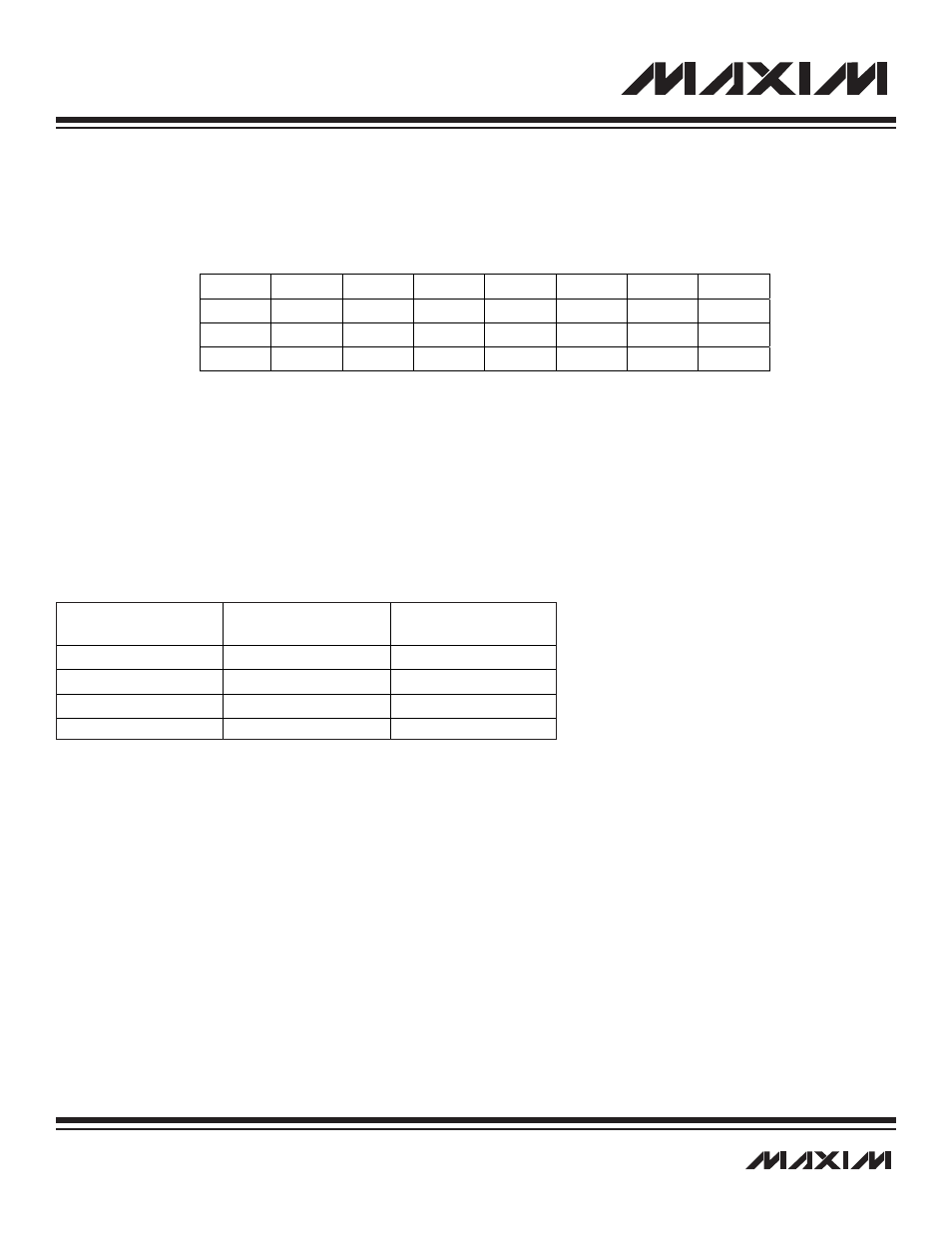
Bit #
7
6
5
4
3
2
1
0
Name
TAP
—
CDA1
CDA0
UPA
ROD
PWL
—
Reset
1
0
0
0
0
0
1
0
Access
rw
r
rw
rw
rw
rw
rw
r
r = read, w = write
Note: Bit 1 (PWL) is set to 1 on a power-on reset only.
CDA[1:0]
BYTE MODE
ACTIVE PAGE
WORD MODE
ACTIVE PAGE
00
P0
P0 and P1
01
P1
P0 and P1
10
P2
P2 and P3
11
P3
P2 and P3