3 spi configuration re, 3 spi configuration register (spicf) -9, Table 9-2. spi clocking mode configuration -9 – Maxim Integrated MAXQ7667 User Manual
Page 171: Maxq7667 user’s guide, Table 9-2. spi clocking mode configuration

9-9
___________________________________________________________________________________________________________
MAXQ7667 User’s Guide
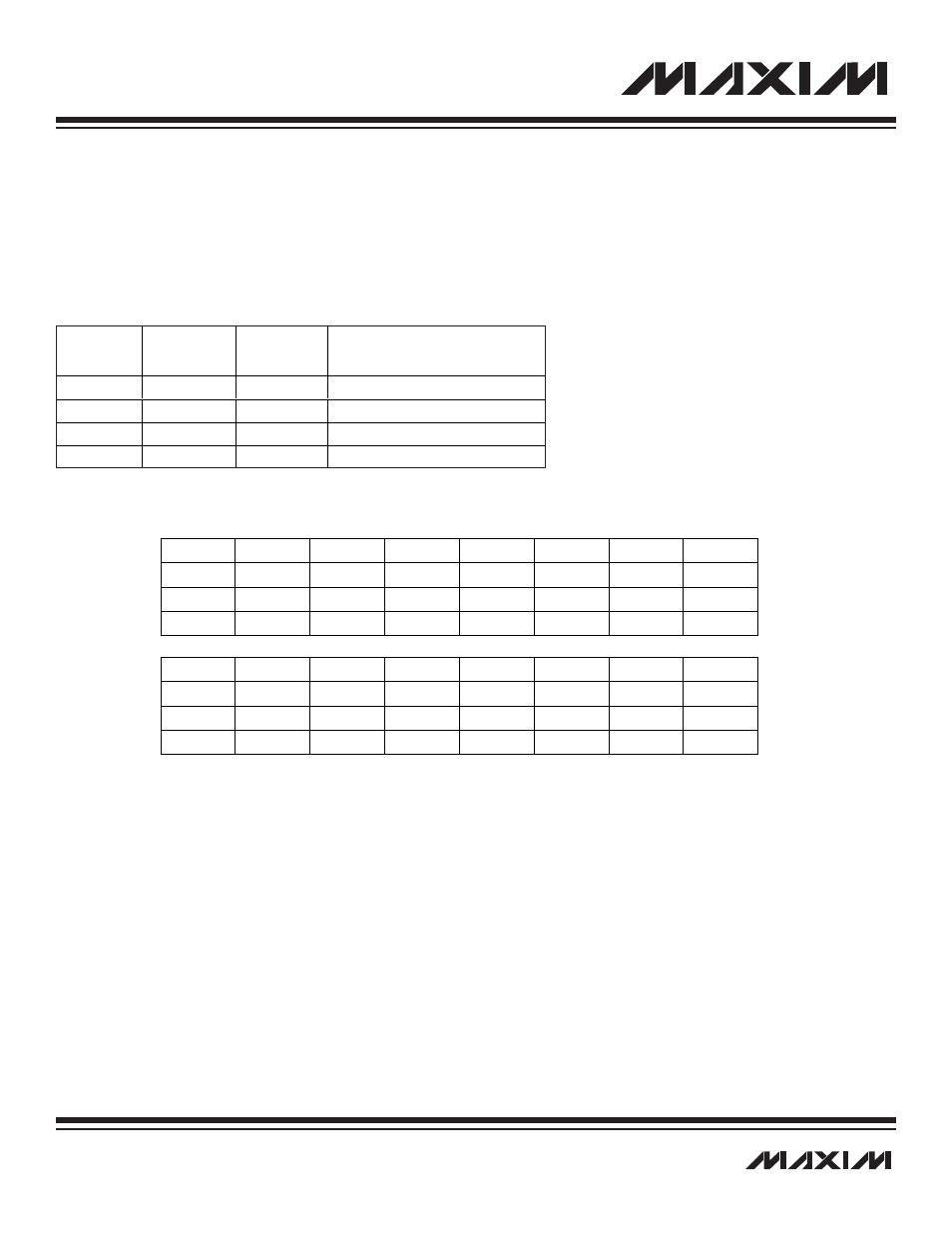
9.1.1.3 SPI Configuration Register (SPICF)
The SPI configuration register (SPICF) contains the port configuration selects. The SPI port supports 8-bit and 16-bit character trans-
fers using the SS pin and an internal bit counter to control transfer completion. Data is shifted on the rising or falling edge of the SCLK
as selected by the clock polarity select (CKPOL) and the clock phase select (CKPHA) bits found in the SPICF. These registers can be
word, byte, or bit accessed.
Table 9-2 shows the four SPI clocking modes supported by the MAXQ7667.
Table 9-2. SPI Clocking Mode Configuration
Register Description:
SPI Configuration Register
Register Name:
SPICF
Register Address:
Module 01h, Index 08h
Bits 15 to 8, 5 to 3: Reserved. Read 0, write ignored.
Bit 7: Enable SPI Interrupt (ESPII). This bit enables any of the SPI interrupt source flags (MODF, WCOL, ROVR, SPIC) to generate
interrupt requests.
0 = SPI interrupt sources disabled.
1 = SPI interrupt sources enabled.
Bit 6: Slave-Active Select (SAS). This bit is used to determine the SS active state. When the SAS is cleared to 0, the SS is active low
and responds to an external low signal. When the SAS is set to 1, the SS pin is active high. Note: The SAS selection is only available
in the enhanced SPI peripheral.
Bit 2: Character Length Select (CHR). This bit determines the character length for an SPI transfer cycle. A character can be 8 bits in
length or 16 bits in length.
0 = 8-bit character length specified.
1 = 16-bit character length specified.
SPI
MODE
CLOCK
POLARITY
(CKPOL)
CLOCK
PHASE
(CKPHA)
TRANSFER METHOD
0
0
0
SPICK rising edge transfer
1
0
1
SPICK falling edge transfer
2
1
0
SPICK falling edge transfer
3
1
1
SPICK rising edge transfer
Bit #
15
14
13
12
11
10
9
8
Name
—
—
—
—
—
—
—
—
Reset
0
0
0
0
0
0
0
0
Access
r
r
r
r
r
r
r
r
Bit #
7
6
5
4
3
2
1
0
Name
ESPII
SAS
—
—
—
CHR
CKPHA
CKPOL
Reset
0
0
0
0
0
0
0
0
Access
rw
rw
r
r
r
rw
rw
rw
r = read, w = write
