1 architecture, 1 burst transmission stage, 2 echo reception – Maxim Integrated MAXQ7667 User Manual
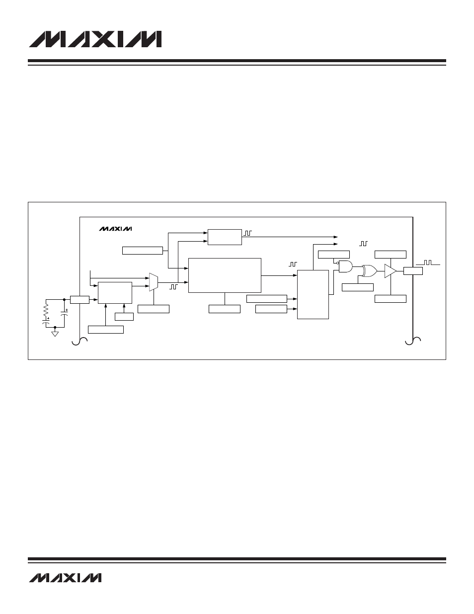
Page 286: 1 architecture -4, 1 burst transmission stage -4, 2 echo reception -4, Figure 17-1. burst transmission stage -4, Maxq7667 user’s guide

17.1.2 Echo Reception
The echo receive path along with the control and data registers are shown in Figure 17-2. The circuit is designed to receive echoes at
the burst frequency, with amplitudes ranging from 10µV
P-P
to 100mV
P-P
. Echo signals between 100mV and 2V are clipped and do not
saturate the receiver. This allows very large echoes to be detected even though information about their magnitude will be lost. To opti-
mize echo reception, the clock used for processing the echo is locked to the burst frequency (B
FREQ
). This guarantees that the cen-
ter frequency of the BPF matches the transducer excitation frequency.
At the beginning of the signal chain is a wideband low-noise amplifier (LNA) with a fixed gain of 40V/V. For debugging purposes the
output of the LNA’s differential output can be monitored with an oscilloscope by connecting it to pins AIN0 and AIN1. For more details
on this capability, see Section 17.5.2.2.
The total gain of the echo receive path is programmable over a 23.5dB range with an average gain step of 0.8dB. Changes in gain are
achieved through a combination of analog and digital techniques. All gain changes settle within one ADC conversion, and any switch-
ing glitches are removed by the LPF. This allows for the implementation of a virtual time variable gain amplifier since gain changes can
be made on the fly.
The 16-bit sigma-delta ADC digitizes the output of the LNA. The ADC’s input sample rate is 80 x B
FREQ
and the output data rate is 10
x B
FREQ
. The output of the ADC’s SINC filter is fed directly to the input of the BPF and can be read from the Echo Envelope Bandpass
Filter Input Data register (BPFI). The reference voltage for the sigma-delta ADC can be provided by two sources: an internal bandgap
reference or an external reference.
17.1 Architecture
17.1.1 Burst Transmission Stage
The MAXQ7667’s burst output excites the transducer when transmitting a burst of ultrasonic sound. The burst output is typically used
to switch an external transistor that drives a high voltage transformer, which excites the transducer.
The burst signal can be derived from either the system clock or from a programmable oscillator (PLL) that is phase locked to the sys-
tem clock. Deriving the burst signal from the system clock limits the burst frequency to one of 16 choices. These 16 frequencies are
generated by integer division of the system clock.
Using the PLL allows a fractional division of the system clock. Fractional division allows the PLL to be programmed for any frequency
within its range with a worst-case programming resolution of 0.13%.
Figure 17-1 shows a block diagram of the echo receive path.
__________________________________________________________________________________________________________
17-4
MAXQ7667 User’s Guide
f
CLOCK-BURST-IN
= f
BURST-CLOCK
DIVIDED BY 12 TO 640, DIVISOR
CONTROLLED BY BDIV
BURST HIGH TIME = BPH/f
CLOCK-BURST-IN
MAXQ7667
PLLF[10:9]:PLL[1:0]
BTRN.9:BTRI
BTRN.8:BGT
BPH.14:BDS
BTRN.[15:12]:BDIV[3:0]
BTRN[7:0]:BCNT[7:0]
BTRN.10:BCKS
BPH.15:BSTT
CLOCK-BURST-IN
PLLF[8:0]
PLL
FPLL = SYSCLK x
(PLLF + 768)/1024
0
1
FILT
BURST
B
FREQ
SYSCLK
(SYSTEM CLOCK)
PLL
CLOCK
BTRN.11:BPOL
PWM
PROGRAMMABLE
DIVIDE BY 2 TO 8
RECV-CLOCK
2mV_DIAG
BPH[9:0]
BURST-CLOCK
R1
24k
Ω
C1
33nF
C2
330pF
Figure 17-1. Burst Transmission Stage
