2 analog interrupt enab, 2 analog interrupt enable register (aie) -6, Maxq7667 user’s guide – Maxim Integrated MAXQ7667 User Manual
Page 238: 2 analog interrupt enable register (aie)

__________________________________________________________________________________________________________
14-6
MAXQ7667 User’s Guide
Bit 3: SAR ADC Start/Busy (SARBY). Setting this bit to 1 starts a conversion if SARS = 111. Reading from this bit reflects the busy
status of the SAR ADC. Changing SARBY from 1 to 0 by software is blocked by hardware.
Bits 2 to 0: SAR ADC Conversion Control Source Select (SARS[2:0]). These bits select the source that initiates SAR ADC
conversions.
000 selects timer 0
001 selects timer 1
010 selects timer 2
011 is reserved
100 selects from ADCCTL pin
101 selects from ADCCTL pin with inverted data
110 selects continuous conversions every 16 clocks
111 selects the SARBY bit
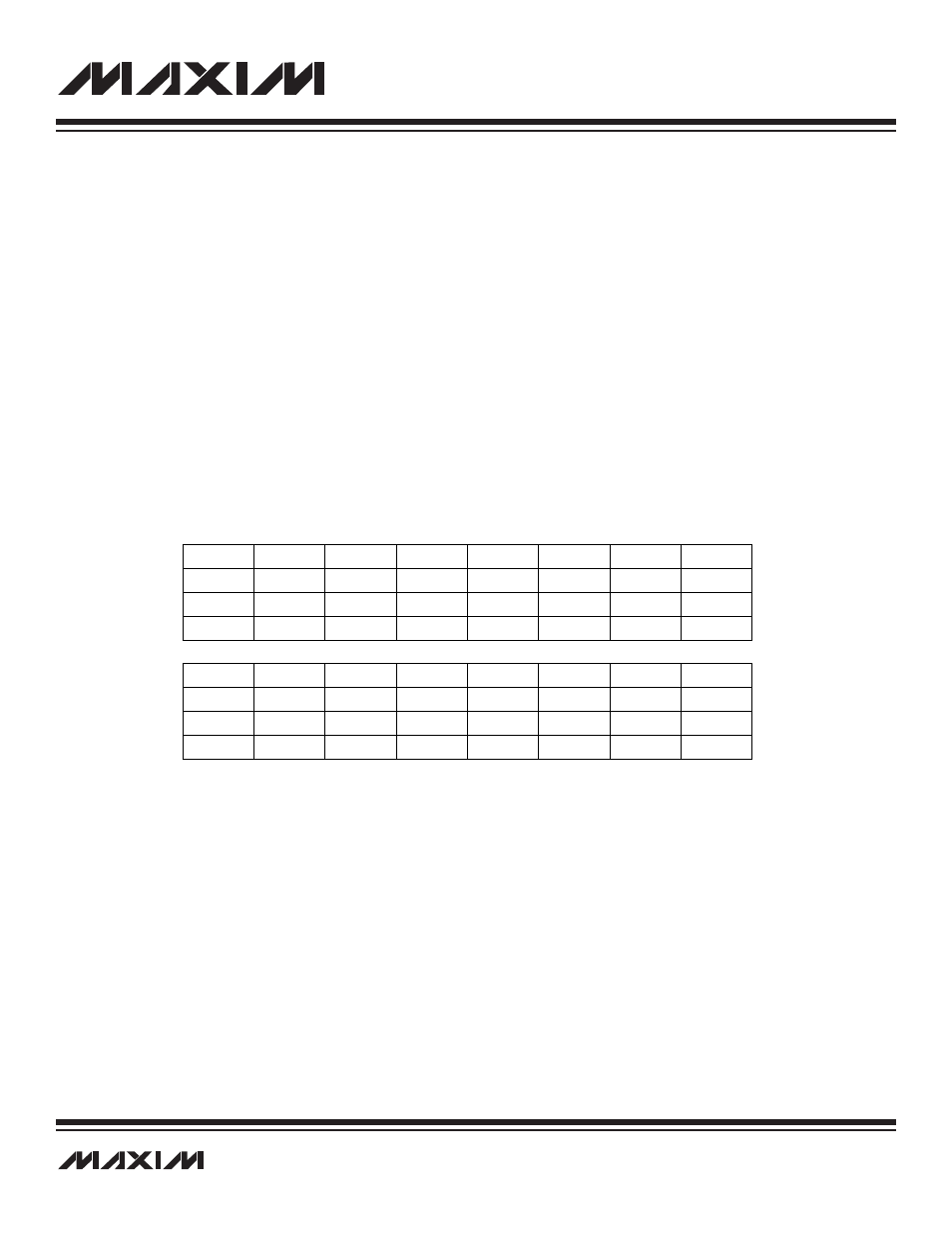
14.3.2 Analog Interrupt Enable Register (AIE)
Register Description:
Analog Interrupt Enable Register
Register Name:
AIE
Register Address:
Module 05h, Index 05h
Bits 15 to 8: Reserved. Read returns 0.
Bit 7: Crystal Oscillator Failure (XTIE). See Section 15 for details on this bit.
Bit 6: DVDDIO Brownout Interrupt Enable (VIBIE). See Section 16 for details on this bit.
Bit 5: DVDD Brownout Interrupt Enable (VDBIE). See Section 16 for details on this bit.
Bit 4: AVDD Brownout Interrupt Enable (VABIE). See Section 16 for details on this bit.
Bit 3: Echo Envelope Comparator Interrupt Enable (CMPIE). See Section 17 for details on this bit.
Bit 2: Echo Envelope Lowpass Filter FIFO Full Interrupt Enable (LFLIE). See Section 17 for details on this bit.
Bit 1: Echo Envelope Lowpass Filter Output Data Ready Interrupt Enable (LPFIE). See Section 17 for details on this bit.
Bit 0: SAR ADC Data Ready Interrupt Enable (SARIE). A 1 allows an interrupt request to be generated when ADC completes a con-
version and SARRDY bit is 1.
Bit #
15
14
13
12
11
10
9
8
Name
—
—
—
—
—
—
—
—
Reset
0
0
0
0
0
0
0
0
Access
r
r
r
r
r
r
r
r
Bit #
7
6
5
4
3
2
1
0
Name
XTIE
VIBIE
VDBIE
VABIE
CMPIE
LFLIE
LPFIE
SARIE
Reset
0
0
0
0
0
0
0
0
Access
rw
rw
rw
rw
rw
rw
rw
rw
r = read, w = write
Note: AIE is cleared to 0000h on all forms of reset.
