18 data pointer control, 18 data pointer control register (dpc) -16, Maxq7667 user’s guide – Maxim Integrated MAXQ7667 User Manual
Page 60: 18 data pointer control register (dpc)

__________________________________________________________________________________________________________
4-16
MAXQ7667 User’s Guide
4.1.18 Data Pointer Control Register (DPC)
Register Description:
Data Pointer Control Register
Register Name:
DPC
Register Address:
Module 0Eh, Index 04h
Bits 15 to 5: Reserved. Read 0, write ignored.
Bit 4: Word/Byte Select 2 (WBS2). This bit selects access mode for BP[OFFS]. When WBS2 is set to logic 1, the BP[OFFS] is oper-
ated in word mode for data memory access; when WBS2 is cleared to logic 0, BP[OFFS] is operated in byte mode for data memory
access.
Bit 3: Word/Byte Select 1 (WBS1). This bit selects access mode for DP[1]. When WBS1 is set to logic 1, the DP[1] is operated in word
mode for data memory access; when WBS1 is cleared to logic 0, DP[1] is operated in byte mode for data memory access.
Bit 2: Word/Byte Select 0 (WBS0). This bit selects access mode for DP[0]. When WBS0 is set to logic 1, the DP[0] is operated in word
mode for data memory access; when WBS0 is cleared to logic 0, DP[0] is operated in byte mode for data memory access.
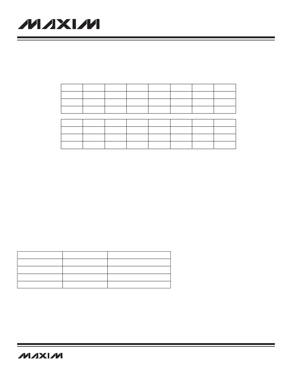
Bits 1 and 0: Source Data Pointer Select Bits 1 and 0 (SDPS[1:0]). These bits select one of the three data pointers as the active
source pointer for the load operation. A new data pointer must be selected before being used to read data memory (see table below).
These bits default to 00b but do not activate DP[0] as an active source pointer until the SDPS bits are explicitly cleared to 00b or the
DP[0] register is written by an instruction. Also, modifying the register contents of a data/frame pointer register (DP[0], DP[1], BP, or
OFFS) will change the setting of the SDPS bits to reflect the active source pointer selection.
Bit #
15
14
13
12
11
10
9
8
Name
—
—
—
—
—
—
—
—
Reset
0
0
0
0
0
0
0
0
Access
r
r
r
r
r
r
r
r
Bit #
7
6
5
4
3
2
1
0
Name
—
—
—
WBS2
WBS1
WBS0
SDPS1
SDPS0
Reset
0
0
0
1
1
1
0
0
Access
r
r
r
rw
rw
rw
rw
rw
r = read, w = write
Note: This register is cleared to 001Ch on all forms of reset.
SDPS1
SDPS0
SOURCE POINTER SELECTION
0
0
DP[0]
0
1
DP[1]
1
0
FP (BP[OFFS])
1
1
Reserved (select FP if set)
