11 control register 0 (u, 11 control register 0 (uart) (cnt0) -13, Maxq7667 user’s guide – Maxim Integrated MAXQ7667 User Manual
Page 143: 11 control register 0 (uart) (cnt0)

8.3.11 Control Register 0 (UART) (CNT0)
Register Description:
Control Register 0
Register Name:
CNT0
Register Address:
Module 03h, Index 14h
Bit 7: Wake Up (WU). This bit enables the host to monitor and control the low-power sleep mode status of the peripheral. It can also
be used to communicate to the host the status of the activity on the LIN bus.
If the host changes this bit from 1 to 0, the peripheral enters a low-power sleep mode. In this mode, most of the clocks internal to the
peripheral are shut down to conserve power. If the peripheral is in the low-power sleep mode and a wake-up condition is detected on
the LIN bus, hardware clears this flag to 0 and issues an interrupt.
If the peripheral is in the low-power sleep state and the host sets this bit to 1, the peripheral issues wake-up requests on the bus
according to the LIN 2.0 specification. If the peripheral is unable to wake up the master, an error is generated and the peripheral returns
to the low-power sleep state.
This bit is automatically cleared to 0 by hardware if the bus is inactive for at least 4 seconds.
Bits 6 and 5: Receive Filter Prescalar Mode 1:0 (FP[1:0]). This field selects the operating mode of the receive filter according to the
following table.
Bit 4: Interrupt Enable (INE). This bit enables the peripheral to issue an interrupt to the host. If this bit is cleared to 0, the interrupt
flags are set but no interrupt is generated.
Bit 3: Automatic Checksum Type (AUT). This bit enables or disables the automatic detection of the checksum type in a LIN frame.
If this bit is set to 1, the peripheral automatically determines the checksum type based on the identifier in the LIN header. If this bit is
cleared to 0, the CK bit (CNT1.7) is used to select the checksum type for the current transmitted or received frame.
Bit 2: Initialization (INIT). This bit is set to 1 by hardware on any system reset. Software must clear it to 0 after all peripheral initial-
ization is complete. Software can also set this bit to 1 at any time to force the peripheral into the reset initialization state. This bit has
no effect in legacy UART mode.
Bit 1: LIN or UART Mode Select (LUN[1:0]). This field selects between LIN master, LIN slave, and legacy UART mode according to
the following table.
8-13
__________________________________________________________________________________________________________
MAXQ7667 User’s Guide
r = read, w = write
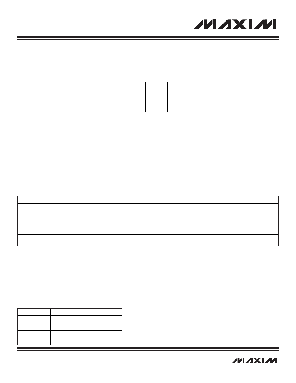
Note: CNT0 is cleared to 8Bh on all forms of reset.
Bit #
7
6
5
4
3
2
1
0
Name
WU
FP1
FP0
INE
AUT
INIT
LUN1
LUN0
Reset
1
0
0
0
1
0
0
0
Access
rw
rw
rw
rw
rw
rw
rw
rw
FP[1:0]
MODE
00
Filter disabled.
01
In this mode, the filter can reject a noise pulse up to 2 system clock cycles wide. A total of 3 clock cycles of latency are added to the receive
filter output.
10
In this mode, the filter can reject a noise pulse up to 4 system clocks wide. A total of 7 clock cycles of latency are added to the receive filter
output.
11
In this mode, the filter can reject a noise pulse up to 6 system clocks wide. A total of 11 clock cycles of latency are added to the receive filter
output.
LUN[1:0]
MODE
00
Legacy UART Mode (default)
01
Legacy UART Mode
10
LIN Master Mode
11
LIN Slave Mode
