3 debug engine operation, 1 background mode opera, 3 debug engine operation -10 – Maxim Integrated MAXQ7667 User Manual
Page 208: 1 background mode operation -10, Maxq7667 user’s guide, 1 background mode operation
_________________________________________________________________________________________________________
12-10
MAXQ7667 User’s Guide
12.3 Debug Engine Operation
To enable a communication link between the host and the MAXQ7667 debug engine, the debug instruction (010b) must be loaded into
the TAP instruction register using the IR-scan sequence (see Section 11). Once the instruction is latched in the instruction parallel buffer
(IR[2:0]) and is recognized by the TAP controller in the update-IR state, the 10-bit data shift register is activated as the communication
channel for DR-scan sequences. The TAP instruction register retains the debug instruction until a new instruction is shifted via an IR-
scan or the TAP controller returns to the test-logic-reset state.
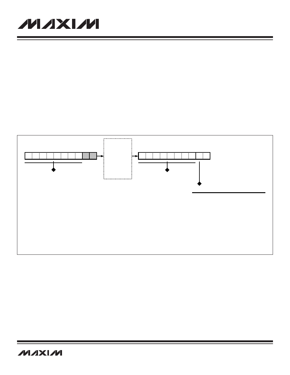
The host now can transmit and receive serial data through the 10-bit data shift register that exists between the TDI input and TDO out-
put during DR-scan sequences. All background and debug mode communication (commands, data input/output, and status) occurs via
this serial channel. Each 10-bit exchange of data between the host and the MAXQ7667 internal hardware is composed of two status bits
and a single byte of command or data. The 10-bit word is always transmitted least significant bit first according to the following format.
The data byte portion of the 10-bit shift register is interfaced directly to the ICDB parallel register. The ICDB register functions as the hold-
ing data register for both transmit and receive operations. On the falling edge of TCK in the update-DR state, the outgoing data is loaded
from the ICDB parallel register to the outgoing data register, while the incoming shift register data is latched in the ICDB parallel register.
12.3.1 Background Mode Operation
When the instruction register is loaded with the debug instruction (IR[2:0] = 010b), the host can communicate with the MAXQ7667 in
a background mode using TAP DR-scan sequences without disturbing CPU operation. Note, however, that JTAG in-system program-
ming also requires use of the 10-bit debug shift register and, if enabled (SPE, PSS[1:0] = 100b), takes precedence over background
mode communication (see Section 13). When operating in background mode, the status bits (Figure 12-2) are always cleared to 00b
(nondebug), which indicates that the MAXQ7667 is ready to receive background mode commands. The host can perform the follow-
ing operations from background mode:
• Read/write internal breakpoint registers (BP0–BP5).
• Read/write internal in-circuit debug registers (ICDC, ICDF, ICDA, ICDD).
• Monitor to determine when a breakpoint match has occurred.
• Directly invoke debug mode.
HOST COMMAND/DATA INPUT
TDI
TDO
MAXQ DATA OUTPUT
00
01
10
11
MAXQ
0
9
X
X
0
9
s1:s0
STATUS/CONDITION
NONDEBUG. DEFAULT CONDITION,
BACKGROUND MODE, OR DEBUG
ENGINE INACTIVE.
DEBUG IDLE. DEBUG ENGINE IS
READY TO RECEIVE DATA FROM THE
HOST (COMMAND, DATA).
DEBUG BUSY. DEBUG ENGINE IS
BUSY WITHOUT VALID DATA (i.e., ROM
CODE EXECUTION, TRACE OPERATIONS).
DEBUG VALID. DEBUG ENGINE IS
BUSY WITH VALID DATA.
Figure 12-2. Data Transmit and Receive During DR-Scan Sequence