1 5v regulator with ext, 1 depletion mode fet, 1 5v regulator with external pass transistor -10 – Maxim Integrated MAXQ7667 User Manual
Page 276: 1 depletion mode fet as the pass device -10, Maxq7667 user’s guide, 1 5v regulator with external pass transistor

_________________________________________________________________________________________________________
16-10
MAXQ7667 User’s Guide
16.3.1 5V Regulator with External Pass Transistor
The 5V supply (DVDDIO) for the MAXQ7667 can be economically obtained from a higher voltage supply through the use of a few exter-
nal components. The MAXQ7667 has an internal error amplifier that compares DVDDIO to a fixed voltage reference. The output of the
error amplifier can be used to control an external pass transistor and thus create a regulated 5V supply. A capacitor from DVDDIO to
ground supplies current for fast transient loads. The largest capacitor that can be used is 0.47µF. Larger capacitors degrade the loop
stability. This capacitor and the pass transistor should be placed as close as practical to the DVDDIO pin.
The output of the error amplifier has a voltage range of 2.0V to DVDDIO - 0.1V. Depending on the control voltage needed at the base
or gate of the pass transistor, an external level shifter may be necessary. Level shifting is easily accomplished with a resistor and a few
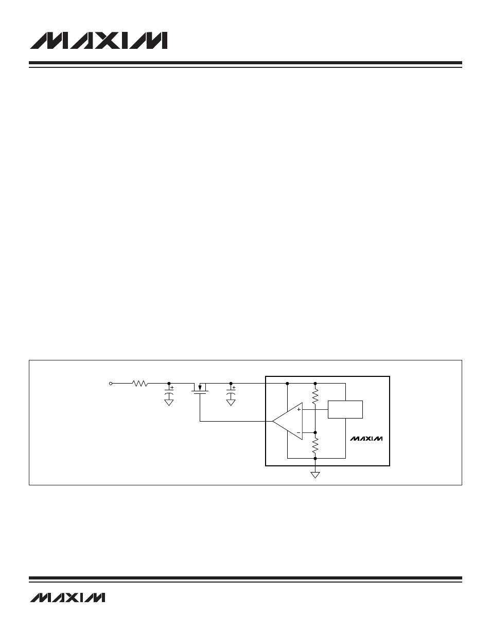
diodes. Figure 16-4 and Figure 16-5 show the use of three types of pass transistors: a depletion mode FET, a bipolar Darlington tran-
sistor, and an enhancement mode FET.
All three figures contain an optional RC filter (R2 and C2) between V
IN
and the pass transistor. This filter is not necessary if V
IN
is a
“clean” voltage. However, adding this filter is recommended if there are transients or RF noise on V
IN
. R2 has a suggested value of
10
Ω, but a lower value may be used if a smaller voltage drop across R2 is needed.
16.3.1.1 Depletion Mode FET as the Pass Device
The depletion mode FET is the simplest configuration. The device is normally on, which allows the MAXQ7667 to power-up and go into
regulation mode. The depletion mode FET provides a built-in current-limiting mechanism, and also offers low dropout since the gate
voltage does not limit the dropout voltage.
There are only three restrictions on the choice of a depletion mode FET as the series pass device. The first restriction is that the device
be able to supply the desired maximum load current when the GATE5 output is at its maximum. Note that I
DSS
is usually specified at
V
GS
= 0V instead of V
GS
= -0.1V, which is the maximum (most on) condition realized with the MAXQ7667. Temperature effects also
must be considered. The transistor must be able to supply enough current over the entire temperature range when V
GS
= -0.1V.
The second restriction is that the GATE5 voltage must be able to turn the FET off. When at V
GS
= -3V, I
D
must be less than the mini-
mum possible supply current. This can be as low as a few µA if the MAXQ7667 is placed in a standby configuration.
The third restriction is that the pole formed by the C
ISS
of the FET and the output resistance of the error amp should be greater than
10 times the error amplifier’s gain bandwidth product. This third criterion is not a problem for most transistors.
A depletion mode FET that works well with the MAXQ7667 is the BSP129.
Figure 16-4. DVDDIO Using a Depletion Mode Pass Transistor
MAXQ7667
R2
10
Ω
ERROR
AMP
VOLTAGE
REFERENCE
DVDDIO
V
IN
5V
Q1
C1
0.1
µF
GATE5
C2
0.1
µF
