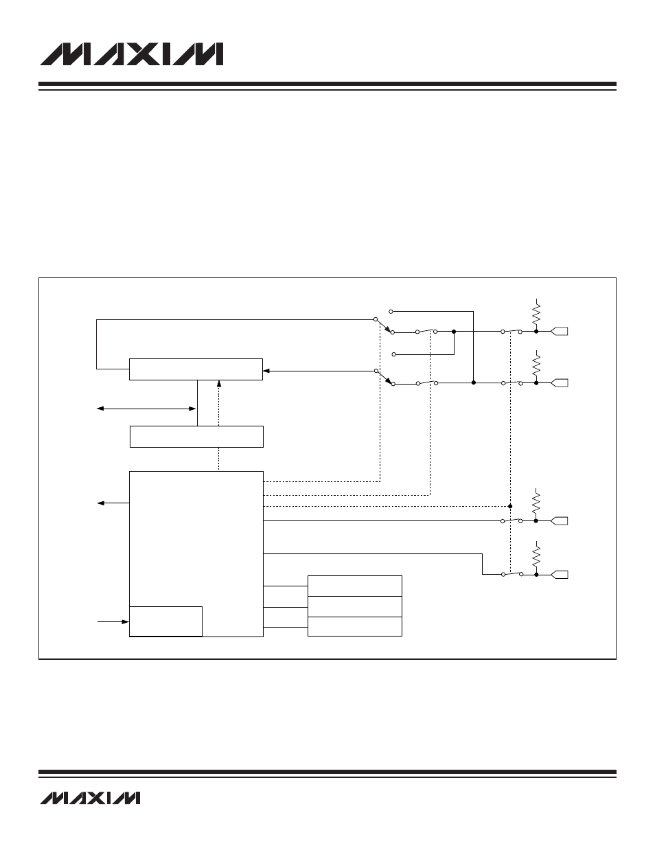
1 architecture, 1 architecture -4, Figure 9-2. spi port functional diagram -4 – Maxim Integrated MAXQ7667 User Manual
Page 166: Maxq7667 user’s guide

___________________________________________________________________________________________________________
9-4
MAXQ7667 User’s Guide
9.1 Architecture
The MAXQ7667 contains a shift register, an independent read buffer, a programmable baud-rate generator, and numerous flags to con-
trol and check the status of the port through interrupts or in a polled fashion. The SPI port shift register handles both transmit and receive
data transfers. The read path is double buffered to free up the shift register for the next SPI transfer. Once a SPI read transfer is com-
plete, data is loaded into the read buffer and the SPI port is ready to accept another character for input or output. The SPI port is single
buffered in the transmit direction. The SPI port should not be written to until a previous transfer is completed as signaled by the SPI trans-
fer complete flag (SPIC) found in the SPI control register (SPICN). A data overrun occurs if the previous character is not read out of the
data buffer before the next incoming character is completely shifted into the port. The SPI data buffer register (SPIB) in the SFR bank
provides access for both transmit and receive data for the CPU. The
maximum data rate of the SPI port is:
• 1/2 of SYSCLK for master mode
• 1/8 of SYSCLK for slave mode
Figure 9-2. SPI Port Functional Diagram
MOSI (P1.4)
SS (P1.7)
SCLK (P1.6)
SHIFT REGISTER
MSB (15)
LSB (0)
SHIFT CLOCK
MASTER/SLAVE SELECT
SPI ENABLE
MASTER
IOVDD
IOVDD
MASTER
SLAVE
IOVDD
IOVDD
SLAVE
READ BUFFER (SPIB)
SPI CONTROL UNIT
/2 MASTER
/8 SLAVE
SYSCLK
SPI INTERRUPT
SFR DATA BUS
SPI CONTROL REG (SPICN)
7
0
SPI CONFIG REG (SPICF)
SPI CLOCK REG (SPICK)
MISO (P1.5)
