1 spi status and control, 1 spi status and control registers -5, Table 9-1. spi port i/o pins -5 – Maxim Integrated MAXQ7667 User Manual
Page 167: Maxq7667 user’s guide, Table 9-1. spi port i/o pins, 1 spi status and control registers
9-5
___________________________________________________________________________________________________________
MAXQ7667 User’s Guide
The MAXQ7667 supports:
• 8-bit or 16-bit character lengths
• Master or slave mode
• Four standard SPI clocking modes
• Programmable master SPICK baud-rate generator
• Configurable SS pin
• MSB first data shifting
• Mode-fault detection
• Data overrun and collision detection
• Interrupt or polled operation
The MAXQ7667 does not support:
• Free-running SPICK and frame sync transfer modes
• LSB first shift
Peripherals used should be compatible with the MAXQ7667-supported SPI modes.
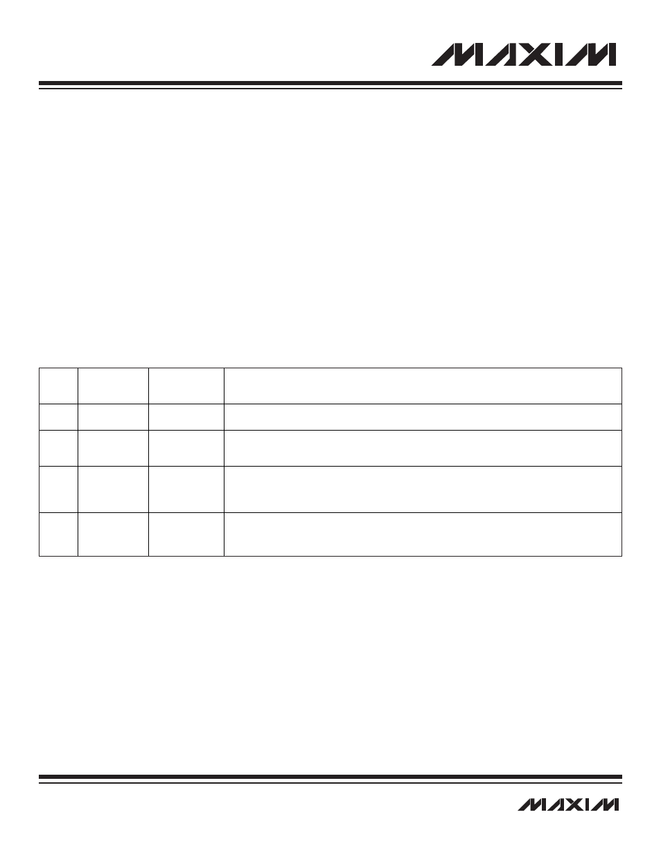
Table 9-1. SPI Port I/O Pins
Additional SS pins in master mode can be defined under firmware control using the digital I/O pins.
9.1.1 SPI Status and Control Registers
Four registers control the SPI port configuration, report status, and operation in the MAXQ7667. These registers are found in the spe-
cial function register bank in Module 1, indexes 6, 7, 8, and 9. The registers are:
• SPI Data Buffer Register (SPIB): Module 1, Index 6
• SPI Control Register (SPICN): Module 1, Index 7
• SPI Configuration Register (SPICF): Module 1, Index 8
• SPI Clock Register (SPICK): Module 1, Index 9
PIN
MULTIPLEXED
WITH PORT
PIN
INTERFACE
SIGNAL
FUNCTION
3
P1.5
MISO
Master In-Slave Out. This signal is an output from an SPI slave device and an input for an SPI master
device. It is used to serially transfer data from the slave to the master. Data is transferred MSB first.
2
P1.4
MOSI
Master Out-Slave In. This signal is an output from an SPI master device and an input for an SPI slave
device. It is used to serially transfer data from a master to a slave device. Data is transferred MSB
first. When in slave mode, the MAXQ default configuration for MISO is an input with a weak pullup.
4
P1.6
SCLK
SPI Clock. This serial clock is an output from an SPI master device and an input for an SPI slave
device. It is used to shift the data between a master and a slave device. The clock polarity select
(CKPOL) and the clock phase select (CKPHA) bits configure the SCLK mode used. The MAXQ7667
supports all four SPI clocking modes.
5
P1.7
SS
Slave Select. The slave-select signal can be configured (SPICF register) as an active-low or active-
high input. In the slave mode, SS is asserted and held low or high (based on its configuration) for the
entire transfer. Shifting out, or in, is stopped when SS is deasserted. This pin can also be configured
to detect a mode-fault condition in master mode.