Maxq7667 user’s guide – Maxim Integrated MAXQ7667 User Manual
Page 250
_________________________________________________________________________________________________________
14-18
MAXQ7667 User’s Guide
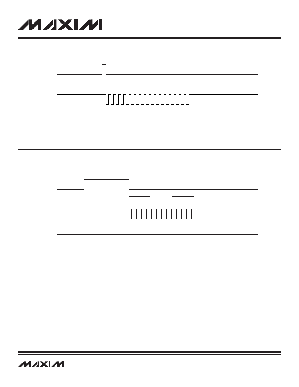
In dual-edged conversions, it is up to the user to provide the required power-up and acquisition delay as explained in Table 14-5.
a) If ADC is in auto shutdown state, a minimum of 2.5µs power-up and acquisition delay is required followed by 13 ADC clock
cycles, for conversion, before the 12-bit result is available.
b) If ADC is not in auto shutdown state, a minimum of 1.5µs acquisition delay is required followed by 13 ADC clock cycles, for
conversion, before the 12-bit result is available.
Figure 14-10 shows dual-edge-controlled ADC conversion when the ADC is in auto shutdown state.
In dual-edge conversion, the power-up and acquisition is triggered by the rising edge of the ADC conversion start source signal
ADC_CNVST (ADC_CNVST is an internal signal generated from a combination of all the three conversion start sources described ear-
lier in this subsection). At the falling edge, the ADC starts conversion and a 12-bit result is written to the ADC result register in 13 ADC
clock cycles. The advantage of dual-edge mode is, depending on the analog input signal’s source impedance, the user can provide
additional acquisition time if required.
Figure 14-10. Dual-Edge ADC Conversion Timing; ADC Previously Off
SARBY
ADCDATA
ADCCLK
ADC_CNVST
DATA (n-1)
DATA (n)
1
13
CONVERSION (n)
POWER-UP AND ACQUISITION
Figure 14-9. Single-Edge ADC Conversion Timing; ADC Previously On
SARBY
1
17
13
ADCDATA
ADCCLK
ADC_CNVST
DATA (n-1)
DATA (n)
ACQUISITION (n)
CONVERSION (n)