Maxim Integrated MAXQ Family User Manual
Maxq family user’s guide
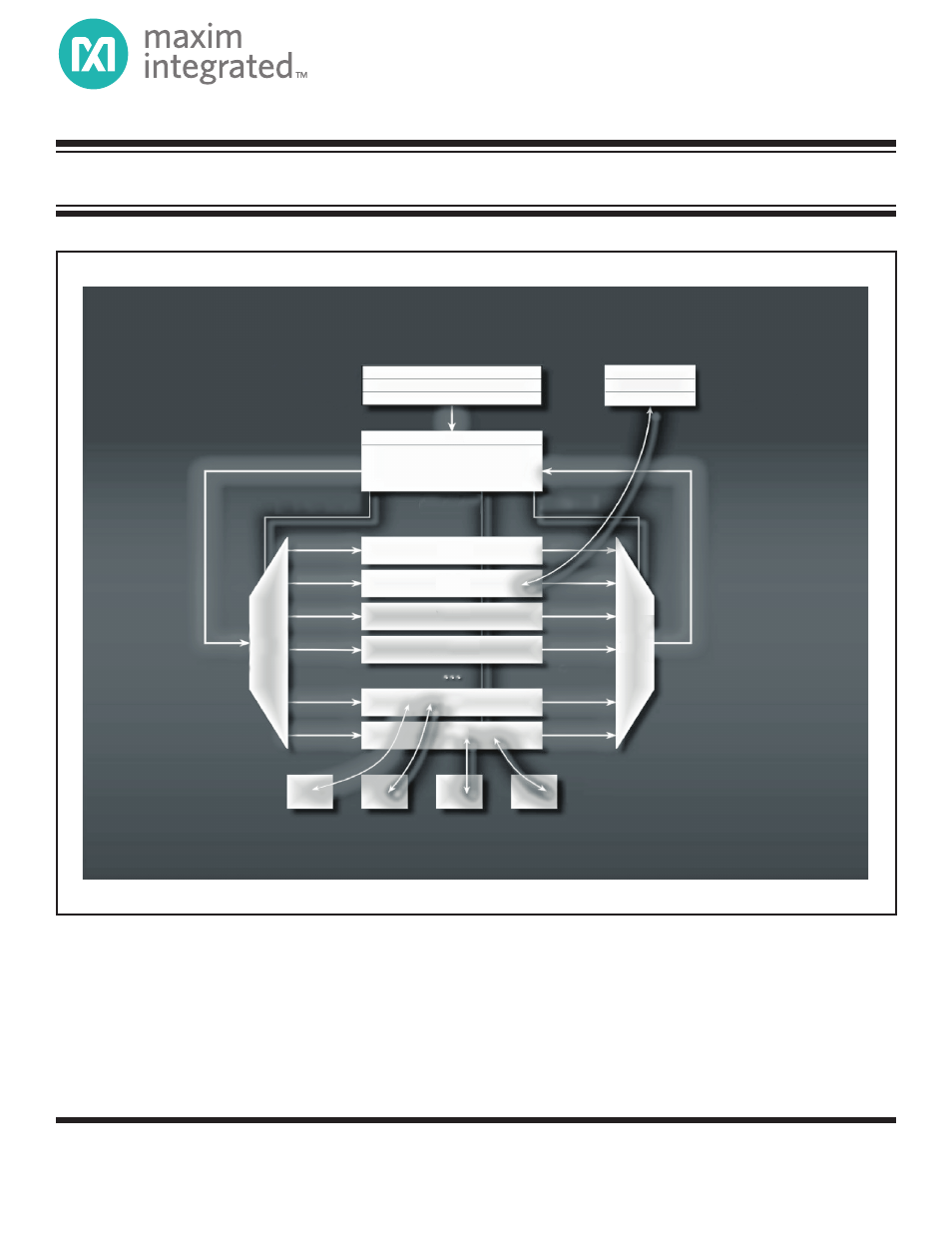
Functional Diagrams
Pin Configurations appear at end of data sheet.
Functional Diagrams continued at end of data sheet.
UCSP is a trademark of Maxim Integrated Products, Inc.
For pricing, delivery, and ordering information, please contact Maxim Direct
at 1-888-629-4642, or visit Maxim’s website at www.maximintegrated.com.
MAXQ FAMILY USER’S GUIDE
Rev: 6; 9/08
Data
Memory
I/O
Source
IR
1:16
16:1
Instruction
Decoder
IP
DP
SP
ALU
I/O
I/O
Program
Memory
Destination
Note: The MAXQ Family User's Guide should be used in conjunction with the data sheet(s) for MAXQ microcontrollers.
Table of contents
Document Outline
- TABLE OF CONTENTS:
- SECTION 1: OVERVIEW
- SECTION 2: ARCHITECTURE
- SECTION 3: PROGRAMMING
- SECTION 4: SYSTEM REGISTER DESCRIPTIONS
- 4.1 Accumulator Pointer Regi...
- 4.2 Accumulator Pointer Cont...
- 4.3 Processor Status Flags R...
- 4.4 Interrupt and Control Re...
- 4.5 Interrupt Mask Register ...
- 4.6 System Control Register ...
- 4.7 Interrupt Identification...
- 4.8 System Clock Control Reg...
- 4.9 Watchdog Control Registe...
- 4.10 (MAXQ10) Accumulator n ...
- 4.11 (MAXQ20) Accumulator n ...
- 4.12 Prefix Register (PFX[n]...
- 4.13 Instruction Pointer Reg...
- 4.14 Stack Pointer Register ...
- 4.15 Interrupt Vector Regist...
- 4.16 Loop Counter 0 Register...
- 4.17 Loop Counter 1 Register...
- 4.18 Frame Pointer Offset Re...
- 4.19 Data Pointer Control Re...
- 4.20 General Register (GR, E...
- 4.21 General Register Low By...
- 4.22 Frame Pointer Base Regi...
- 4.23 General Register Byte-S...
- 4.24 General Register High B...
- 4.25 General Register Sign E...
- 4.26 Frame Pointer Register ...
- 4.27 Data Pointer 0 Register...
- 4.28 Data Pointer 1 Register...
- SECTION 5: PERIPHERAL REGISTER MODULES
- SECTION 6: GENERAL-PURPOSE I/O MODULE
- SECTION 7: TIMER/COUNTER 0 MODULE
- SECTION 8: TIMER/COUNTER 1 MODULE
- SECTION 9: TIMER/COUNTER 2 MODULE
- 9.1 Timer 2
- 9.2 Modes of Operation
- 9.3 Timer 2 Capture Applicat...
- 9.4 Timer/Counter 2 Peripher...
- 9.5 Low-Speed Infrared Trans...
- 9.6 IR Peripheral Register
- SECTION 10: SERIAL I/O MODULE
- SECTION 11: SERIAL PERIPHERAL INTERFACE (SPI) MODULE
- SECTION 12: HARDWARE MULTIPLIER MODULE
- SECTION 13: 1-Wire BUS MASTER
- SECTION 14: REAL-TIME CLOCK MODULE
- SECTION 15: TEST ACCESS PORT (TAP)
- SECTION 16: IN-CIRCUIT DEBUG MODE
- SECTION 17: IN-SYSTEM PROGRAMMING (JTAG)
- SECTION 18: MAXQ FAMILY INSTRUCTION SET SUMMARY
- ADD/ADDC src
- AND src
- AND Acc.
- {L/S}CALL src
- CMP src
- CPL
- CPL C
- {L/S}DJNZ LC[n], src
- {L/S} JUMP src
- {L/S}JUMP C/{L/S}JUMP NC, sr...
- MOVE dst, src
- MOVE Acc., C
- MOVE C, Acc.
- MOVE C, src.
- MOVE C, #0
- MOVE C, #1
- MOVE dst., #0
- MOVE dst., #1
- NEG
- OR src
- OR Acc.
- POP dst
- POPI dst
- PUSH src
- RET
- RET C/RET NC, RET Z/RET NZ, ...
- RETI
- RETI C/RETI NC, RETI Z/RETI ...
- RL/RLC
- RR/RRC
- SLA/SLA2/SLA4
- SR/SRA/SRA2/SRA4
- SUB/SUBB src
- XCH
- XCHN
- XOR src
- XOR Acc.
- REVISION HISTORY