7 type 2 timer input clo, 8 type 2 timer compare a, 1 a simple waveform ou – Maxim Integrated MAXQ7667 User Manual
Page 117: 7 type 2 timer input clock selection -23, 8 type 2 timer compare application examples -23, 1 a simple waveform output -23, Figure 6-5. type 2 timer clock -23, Figure 6-6. simple waveform output -23, Maxq7667 user’s guide, 7 type 2 timer input clock selection

6-23
__________________________________________________________________________________________________________
MAXQ7667 User’s Guide
6.7.7 Type 2 Timer Input Clock Selection
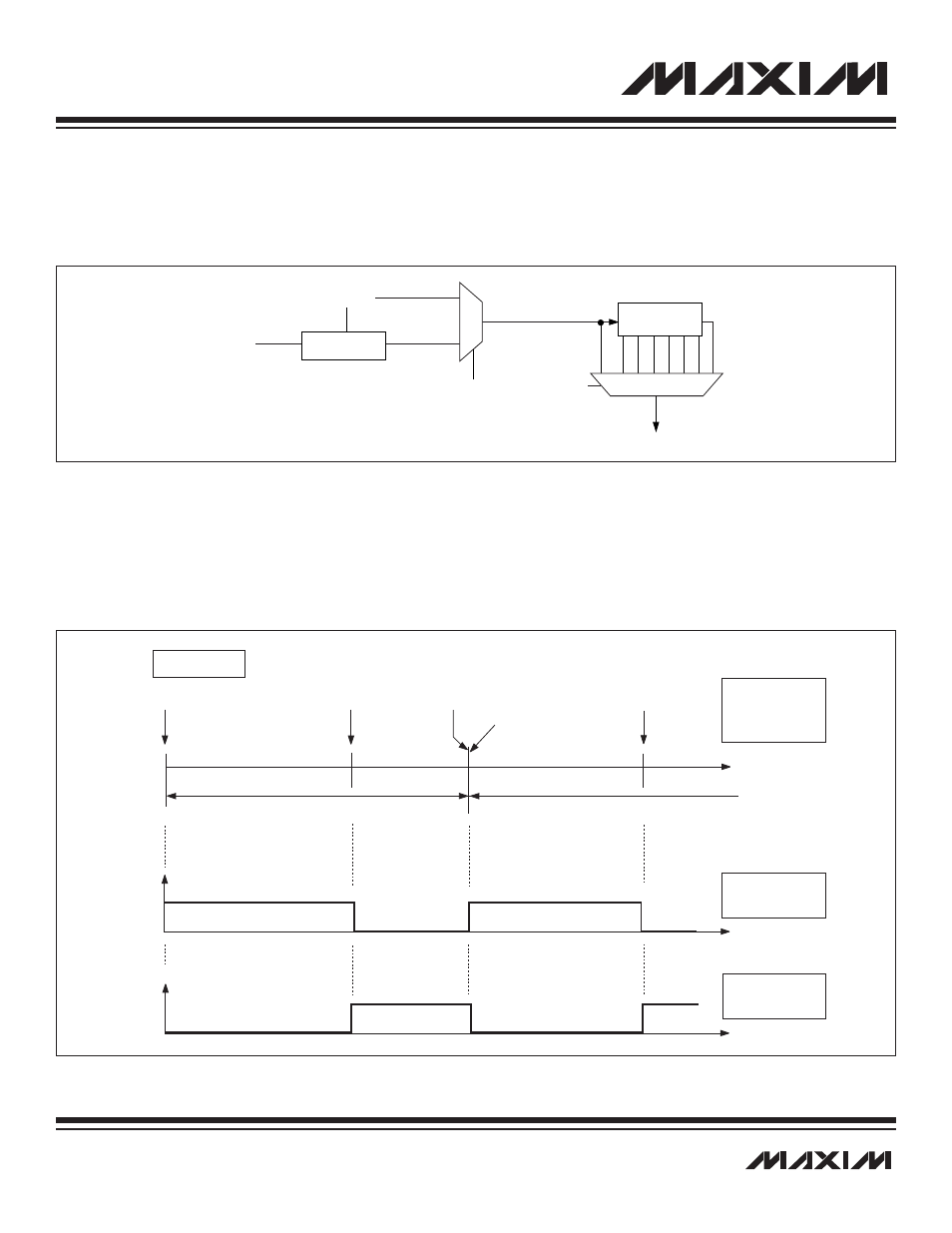
The Type 2 timer clock source is illustrated in Figure 6-5. The timer input clock is selected by the T2CI bit while the clock prescale is deter-
mined by the T2DIV bits in the T2CFGx register. Note that when T2CI is configured to a 1, the alternate clock source (32kHz) is sampled
by the current system clock selection. The maximum frequency that can be sampled on the alternate clock frequency is (system clock/4).
6.7.8 Type 2 Timer Compare Application Examples
6.7.8.1 A Simple Waveform Output
The following code will output a waveform on T2P0 and T2P0B of the Type 2 timer that has a duty cycle of 2/3 on the primary pin and
1/3 on the secondary pin. The T2V0 and T2R0 could have been loaded with 0s as well, without affecting the duty cycle but it would
change the period and hence the frequency. The code can be enhanced to dynamically change the duty cycle and the frequency of
the output signal by continuously updating the values of T2R0 and T2V0 in the body of the code.
INTERNAL
OPERATION OF
THE TIMER
2ND CYCLE
1ST CYCLE
OUTPUT ON THE
PRIMARY PIN
NOT TO SCALE
OUTPUT ON THE
SECONDARY PIN
START T2V0 = 4000h
COMPARE
T2V0 = T2C0 =
C000h
COMPARE
T2V0 = T2C0 =
C000h
OVERFLOW
T2V0 = FFFFh
RELOAD:
T2V0 = 4000h
Figure 6-6. Simple Waveform Output
T2CI
32kHz
T2DIV[2:0]
SYSTEM CLOCK
T2CLK
EDGE DETECTION
DIVIDE-BY-N
PRESCALE
Figure 6-5. Type 2 Timer Clock
