2 architecture, 2 architecture -6, Maxq7667 user’s guide – Maxim Integrated MAXQ7667 User Manual
Page 11
___________________________________________________________________________________________________________
2-6
MAXQ7667 User’s Guide
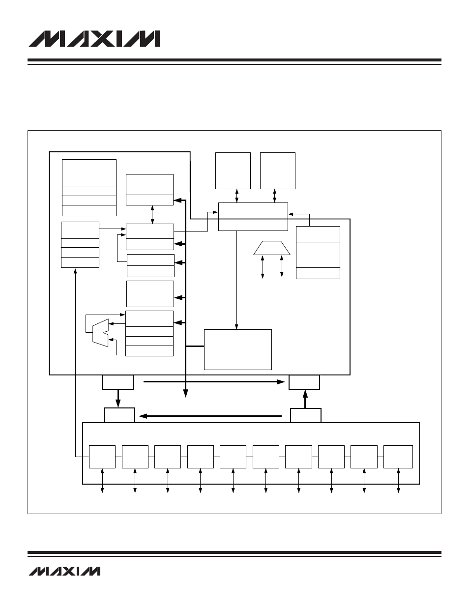
2.2 Architecture
The MAXQ7667 architecture is designed to be modular and expandable. Top-level instruction decoding is extremely simple and based
on transfers to and from registers. The registers are organized into functional modules, which are in turn divided into the system reg-
ister and peripheral register groups. Figure 2-2 illustrates the modular architecture.
SYSTEM MODULES/
REGISTERS
PERIPHERAL MODULES/REGISTERS
DATA
MEMORY
dst
STACK
MEMORY
CKCN
WDCN
IC
ADDRESS
GENERATION
IP
SP
IC
LOOP COUNTERS
LC[
η]
IIR
IMR
INTERRUPT
LOGIC
CLOCK CONTROL,
WATCHDOG TIMER
AND POWER MONITOR
BOOLEAN
VARIABLE
MANIPULATION
ACCUMULATORS
(16)
AP
APC
PSF
INSTRUCTION
DECODE
(SRC, DST TRANSPORT
DETERMINATION)
MUX
DATA POINTERS
DP[0], DP[1]
FP =
(BP + OFFS)
DPC
SC
MEMORY MANAGEMENT
UNIT (MMU)
PROGRAM
MEMORY
src
dst
src
GENERAL-
PURPOSE
I/O
TIMERS/
COUNTERS
UART
(LIN)
SPI
ANALOG
HARDWARE
MULTIPLIER
JTAG
DEBUG
ENGINE
SCHEDULE
TIMER
CLOCK
ULTRASONIC
SOUND
MEASUREMENT
Figure 2-2. MAXQ7667 Transport-Triggered Architecture