6 in-circuit debug addr, 7 in-circuit debug data, 6 in-circuit debug address register (icda) -8 – Maxim Integrated MAXQ7667 User Manual
Page 206: 7 in-circuit debug data register (icdd) -8, Maxq7667 user’s guide, 6 in-circuit debug address register (icda), 7 in-circuit debug data register (icdd)

__________________________________________________________________________________________________________
12-8
MAXQ7667 User’s Guide
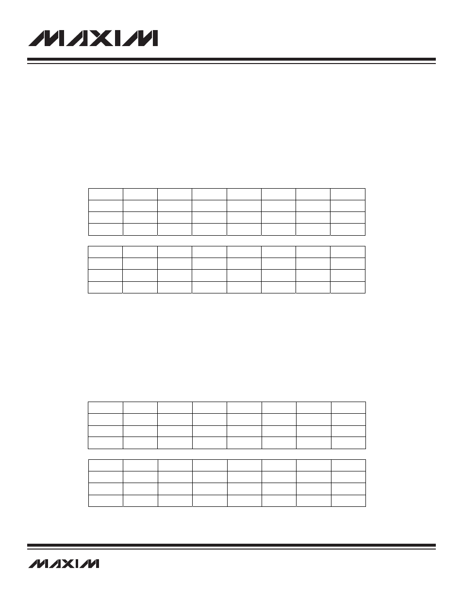
12.2.6 In-Circuit Debug Address Register (ICDA)
The debug engine uses the ICDA register to store addresses so that ROM code may view that information. This register is also used
by the debug engine as a mask register to mask out don’t care bits in the ICDD register when BP5 is used as a register breakpoint.
When a bit in this register is set to 1, the corresponding bit location in the ICDD register is compared to the data being written to the
destination register to determine if a break should be generated. When a bit in this register is cleared, the corresponding bit in the
ICDD register are don’t cares and are not compared against the data being written. When all bits in this register are cleared, any updat-
ed data pattern causes a break when the BP5 register matches the destination register address of the current instruction. This regis-
ter is cleared to 0000h after a power-on reset or a test-logic-reset TAP state.
Register Description:
In-Circuit Debug Address Register
Register Name:
ICDA
Register Address:
Module 02h, Index 1Dh
Bits 15 to 0: In-Circuit Debug Address Register Bits 15:0 (ICDA[15:0])
12.2.7 In-Circuit Debug Data Register (ICDD)
The debug engines uses the ICDD register to store data/read count so that ROM code can view that information. The debug engine also
uses this register as a data register for content matching when BP5 is used as a register breakpoint. In this case, only data bits in this
register with their corresponding mask bits in the ICDA register set are compared with the updated destination data to determine if a
break should be generated. This register is cleared to 0000h after a power-on reset and or a test-logic-reset sequence TAP state.
Register Description:
In-Circuit Debug Data Register
Register Name:
ICDD
Register Address:
Module 02h, Index 1Eh
Bits 15 to 0: In-Circuit Debug Data Register Bits 15:0 (ICDD[15:0])
Bit #
15
14
13
12
11
10
9
8
Name
ICDA15
ICDA14
ICDA13
ICDA12
ICDA11
ICDA10
ICDA9
ICDA8
Reset
0
0
0
0
0
0
0
0
Access
r
r
r
r
r
r
r
r
Bit #
7
6
5
4
3
2
1
0
Name
ICDA7
ICDA6
ICDA5
ICDA4
ICDA3
ICDA2
ICDA1
ICDA0
Reset
0
0
0
0
0
0
0
0
Access
r
r
r
r
r
r
r
r
r = read
Bit #
15
14
13
12
11
10
9
8
Name
ICDD15
ICDD14
ICDD13
ICDD12
ICDD11
ICDD10
ICDD9
ICDD8
Reset
0
0
0
0
0
0
0
0
Access
r
r
r
r
r
r
r
r
Bit #
7
6
5
4
3
2
1
0
Name
ICDD7
ICDD6
ICDD5
ICDD4
ICDD3
ICDD2
ICDD1
ICDD0
Reset
0
0
0
0
0
0
0
0
Access
r
r
r
r
r
r
r
r
r = read
