2 gpio port pins, 2 gpio port pins -4, Table 5-1. port p0 pins -4 – Maxim Integrated MAXQ7667 User Manual
Page 79: Table 5-2. port p1 pins -4, Maxq7667 user’s guide, Table 5-2. port p1 pins, Table 5-1. port p0 pins
___________________________________________________________________________________________________________
5-4
MAXQ7667 User’s Guide
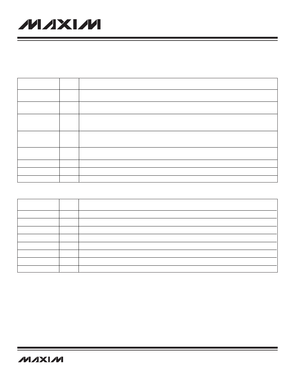
5.1.2 GPIO Port Pins
The MAXQ7667 port P0 and P1 pins are summarized in Table 5-1 and Table 5-2.
PORT P1
SIGNALS
PIN
FUNCTION
P1.0/TD0
46
Digital GPIO and JTAG Serial Data Output. As TDO this pin is the JTAG serial test data output.
P1.1/TMS
47
Digital GPIO and JTAG Test Mode Select Input. As TMS this pin is the JTAG test mode select input.
P1.2/TDI
48
Digital GPIO and JTAG. As TDI this pin is the JTAG serial test data input.
P1.3/TCK
1
Digital GPIO and JTAG Serial Clock Input. As TCK this pin is the JTAG serial test clock input.
P1.4/MOSI
2
Digital GPIO and SPI Serial Data I/O. As MOSI this pin is the master out-slave in for the SPI interface.
P1.5/MISO
3
Digital GPIO and SPI Serial Data I/O. As MISO this pin is the master in-slave out for the SPI interface.
P1.6/SCLK
4
Digital GPIO and SPI Serial Clock. As SCLK this pin is the serial clock for the SPI interface.
P1.7/SYNC/SS
5
Digital GPIO, System Timer Sync Input, and SPI Port Slave Select. As SYNC this pin resets the system timer.
Table 5-2. Port P1 Pins
PORT P0
SIGNALS
PIN
FUNCTION
P0.0/URX
9
Digital GPIO and UART Receive Data Input. As URX this pin is the receive data input of the UART, which can
(optionally) be connected to RXD of a LIN transceiver.
P0.1/UTX
10
Digital GPIO and UART Transmit Data Output. As UTX this pin is the transmit data output of the UART, which can
(optionally) be connected to TXD of a LIN transceiver.
P0.2/TXEN
11
Digital GPIO and UART Transmit. As TXEN the pin can be used to control the transmit enable of an external driver. This
pin defaults to TXEN any time the UART is used. TXEN is high when the UART is receiving and low when the UART is
transmitting.
P0.3/T0/
ADCCTL
12
Digital GPIO, Timer 0 I/O, and ADC Control Input. As T0 this pin is the primary timer/PWM0 input or output. As
ADCCTL this user-programmable rising or falling edge controls the SAR ADC sampling instant and start of
conversion. Optionally, the other edge can be used to enable the ADC and begin acquiring prior to sampling.
P0.4/T0B
13
Digital GPIO, Timer 0 I/O, and Comparator Output. As T0B this pin is the secondary timer/PWM1 input or output. As
CMPO this pin is the output of the digital comparator for the lowpass filter.
P0.5/T1
14
Digital GPIO and Timer 1 I/O. As T1 this pin is the primary timer/PWM2 input or output.
P0.6/T2
15
Digital GPIO and Timer 2 I/O. As T2 this pin is the primary timer/PWM2 input or output.
P0.7/T2B
16
Digital GPIO and Timer 2 I/O. As T2B this pin is the secondary timer/PWM2 input or output.
Table 5-1. Port P0 Pins