2 sar adc pins, 2 sar adc pins -4, Table 14-1. sar adc module pins -4 – Maxim Integrated MAXQ7667 User Manual
Page 236: Maxq7667 user’s guide, Table 14-1. sar adc module pins
__________________________________________________________________________________________________________
14-4
MAXQ7667 User’s Guide
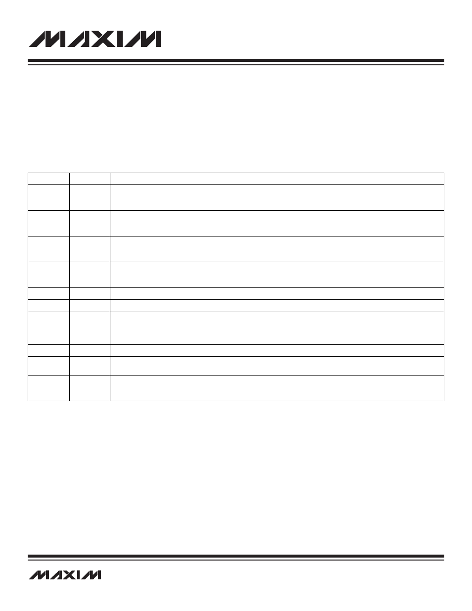
Table 14-1. SAR ADC Module Pins
The ADC gets the reference from three sources: external source REF, internal buffered-bandgap reference that provides 2.5V, and
AVDD. The internal bandgap and reference buffer can be individually disabled, allowing external reference(s) to drive any of these
nodes. All are disabled at power-on to avoid contention if external reference(s) are used. The reference sources are designed to quick-
ly power on and off to minimize power consumption in applications that duty-cycle between run and sleep modes.
14.2 SAR ADC Pins
Table 14-1 shows all the pins in the SAR ADC module.
NAME
PIN
FUNCTION
AIN0
36
Analog Input 0. This ADC input pin can be used for single-ended measurements relative to AGND or for differential
measurement relative to analog input AIN1 (negative side). The active ADC input signal is selectable via the analog
multiplexer.
AIN1
37
Analog Input 1. This ADC input pin can be used for single-ended measurements relative to AGND or for differential
measurement relative to analog input AIN0 (positive side). The active ADC input signal is selectable via the analog
multiplexer.
AIN2
38
Analog Input 2. This ADC input pin can be used for single-ended measurements relative to AGND or for differential
measurement relative to analog input AIN3 (negative side). The active ADC input signal is selectable via the analog
multiplexer.
AIN3
39
Analog Input 3. This ADC input pin can be used for single-ended measurements relative to AGND or for differential
measurement relative to analog input AIN2 (positive side). The active ADC input signal is selectable via the analog
multiplexer.
AIN4
40
Analog Input 4. This ADC input pin can be used for single-ended measurements only relative to AGND.
REFBG
35
Internal 2.5V Reference Output. Connect a minimum value of 0.47µF bypass capacitor to AGND.
REF
34
ADC Reference Input and Reference Buffer Output. This pin is for the ADC reference input. The buffer connected to the
REFBG pin must be disabled to allow the pin to accept an external reference input. Provide a bypass to AGND with a 0.47µF
capacitor. This pin requires a low ESR, which can be done by using two capacitors in parallel instead of one, e.g., a 1µF
capacitor in parallel with a 10nF capacitor instead of just a 1µF capacitor.
AGND
28, 31, 33
Analog Ground. This pin provides the ground reference for all internal analog circuitry.
AVDD
27, 32
Analog Supply Voltage (+3.3V). This pin provides power to all the analog blocks. Connect all AVDD pins to the same point.
Connect to REG3P3 and bypass with a 0.47µF capacitor to ground for self-powered operation.
ADCCTL
12
ADC Control Input. Digital GPIO, Timer 0 I/O, and Port 0.3. As ADCCTL this pin is user programmable; rising or falling
edge controls the SAR ADC sampling instant and start of conversion. Optionally, the other edge can be used to enable the
ADC and begin acquiring prior to sampling. This pin can also be configured as a digital I/O or as a primary timer/PWM I/O.