Table 17-5. integer divisor values -19, Maxq7667 user’s guide, Table 17-5. integer divisor values – Maxim Integrated MAXQ7667 User Manual
Page 301

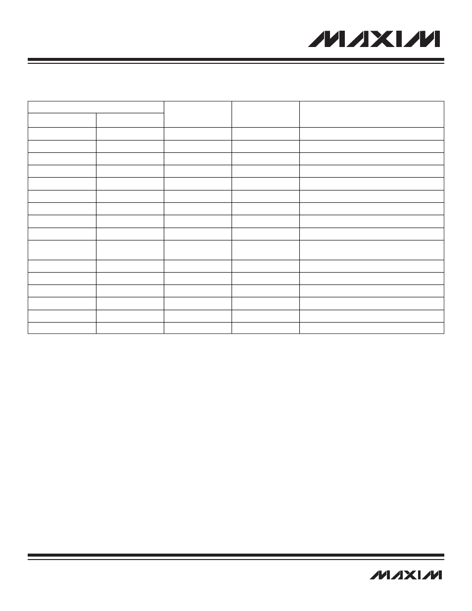
Table 17-5. Integer Divisor Values
The burst clock generated can be controlled and manipulated, in a few ways, before it reaches the output pin BURST.
The polarity of the output signal is controlled by the burst polarity bit, BPOL (BTRN.11). Setting it to 0 would keep the signal normally
low with high going pulses. Setting BPOL to 1 keeps the signal high with low going pulses.
The drive strength of the burst signal is controlled by the burst drive strength bit, BDS (BPH.14). This bit selects the drive strength on
the BURST pin. When the BDS bit is set to 0, the output driver is lower (refer to the datasheet for this value); when set to 1, the output
driver is higher (refer to the data sheet for this value).
The burst signal can be stopped from reaching the BURST pin by setting the burst gate bit, BGT (BTRN.8), to 1. Internally the burst
signal is still available for diagnostic purposes. Setting BGT to 0 allows the burst signal to pass through to the output pin.
The BURST output pin can be set to three-state mode by setting the burst three-state bit, BTRI (BTRN.9) to 1. At power-up, BTRI is set
to 1. This places the BURST output pin in a three-state mode, which prevents large amounts of current from flowing through the exter-
nal transformer while the MAXQ7667 is being initialized. During the initialization process BPOL and the other burst parameters should
be set before BTRI is set to 0, which enables the BURST output pin. A pullup or pulldown resistor should be used to hold the external
transistor in the desired state while the MAXQ7667 is being initialized.
17-19
_________________________________________________________________________________________________________
MAXQ7667 User’s Guide
BDIV
BINARY
HEX
Rdivisor
Bdivisor
NOMINAL BURST FREQUENCY IF
f
Clock-Burst-In
= 16MHz
(kHz)
0000
00
—
12
1333
0001
01
—
16
1000
0010
02
—
20
800
0011
03
—
28
571
0100
04
—
36
444
0101
05
—
48
333
0110
06
—
64
250
0111
07
—
90
178
1000
08
—
120
133
1001
(default)
09
(default)
2
160
100
1010
0A
3
240
66.7
1011
0B
4
320
50
1100
0C
5
400
40
1101
0D
6
480
33.3
1110
0E
7
560
28.6
1111
0F
8
640
25
Note: The burst clock-divide select bit selects the divide ratio between the clock source specified by BCKS and the burst and receive path clocks. Note that
the receive path clock is not active for burst-divide ratios of less than 160. Defaults to 1001 upon reset.
