3 memory organization, 1 program memory, 3 memory organization -10 – Maxim Integrated MAXQ7667 User Manual
Page 15: 1 program memory -10, Maxq7667 user’s guide
__________________________________________________________________________________________________________
2-10
MAXQ7667 User’s Guide
2.2.3 Memory Organization
Beyond the internal register space, memory on the MAXQ7667 microcontroller is organized according to a Harvard architecture, with
a separate address space and bus for program memory and data memory. Stack memory is also separate and is accessed through
a dedicated register set.
To provide additional memory map flexibility, an MMU allows data memory space to be mapped into a predefined program memory seg-
ment, thus affording the possibility of code execution from data memory. Additionally, program memory space can be made accessible
as data space, allowing access to constant data stored in program memory. All memory is internal, and physical memory segments
(other than the stack and register memories) can be accessed as either program memory or as data memory, but not both at once.
2.2.3.1 Program Memory
The MAXQ7667 contains up to 16K x 16 (32KB) of flash memory, which normally serves as program memory. When executing from the
data SRAM or utility ROM, this memory is mapped to data space and can be used for lookup tables and similar functions. Flash mem-
ory mapped into data space can be read from directly, like any other type of data memory. However, writing to flash memory must be
done by calling the in-application functions provided by the utility ROM. The utility ROM provides routines to carry out the necessary
operations (erase, write) on flash memory.
Program memory begins at address 0000h and is contiguous through the internal program memory. The actual size of the on-chip pro-
gram memory available for user application is product dependent. Given a 16-bit program address bus, the maximum program space
is 64KWords. Since the codewords are 16 bits, the program memory is therefore a 64K x 16 linear space.
Program memory is accessed directly by the program fetching unit and is addressed by the Instruction Pointer register. From an imple-
mentation perspective, system interrupts and branching instructions simply change the contents of the Instruction Pointer and force
the op code fetch from a new program location. The Instruction Pointer is direct read/write accessible by the user software; write access
to the Instruction Pointer will force program flow to the new address on the next cycle following the write. The contents of the Instruction
Pointer will be incremented by 1 automatically after each fetch operation. The Instruction Pointer defaults to 8000h, which is the start-
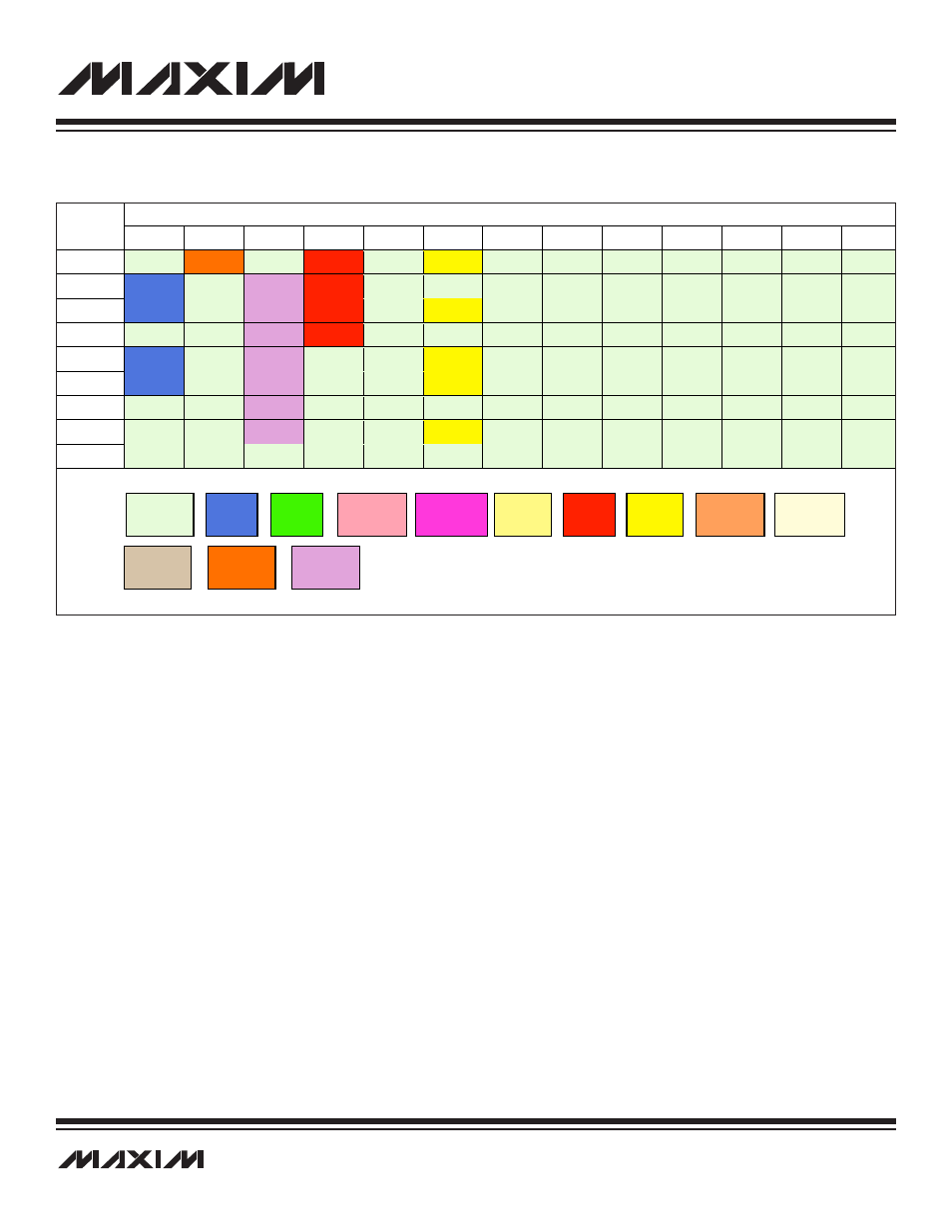
MODULE NAME (BASE SPECIFIER)
REGISTER
INDEX
M0
M1
M2
M3
M4
M5
M8
M9
M11
M12
M13
M14
M15
17h
RCTRM†
SADDR
A2B
18h
PS0
ICDT0
SADEN
19h
PS1
ICDT1
BT
A2D
1Ah
ICDC
TMR
1Bh
PR0
ICDF
A3A
1Ch
PR1
ID0
ICDB
A3B
1Dh
ID1
ICDA
1Eh
ICDD
A3D
1Fh
RESERVED
OR
OPCODE
PORT
PINS
(GPIO)
SPI
INTERRUPT
CONTROL
HARDWARE
MULTIPLIER
TIMERS
UART
(LIN)
ANALOG
I/O
ACC
ARRAY,
CONTROL
OTHER
FUNCTIONS
SCHEDULE
TIMER
TRIM
REGISTER
JTAG
DEBUG
Table 2-2. MAXQ7667 Register Modules (continued)
†The RCTRM register is a read/write register, but on power-up flash restores the factory-trimmed voltage. (Contact Maxim for write capability.)