2 port registers, 1 port 0 output register, 2 port 1 output register – Maxim Integrated MAXQ7667 User Manual
Page 80: 2 port registers -5, 1 port 0 output register (po0) -5, 2 port 1 output register (po1) -5, Maxq7667 user’s guide, 1 port 0 output register (po0), 2 port 1 output register (po1)

5-5
___________________________________________________________________________________________________________
MAXQ7667 User’s Guide
5.2 Port Registers
The following peripheral registers control the general-purpose I/O and external interrupt features specific to the MAXQ7667.
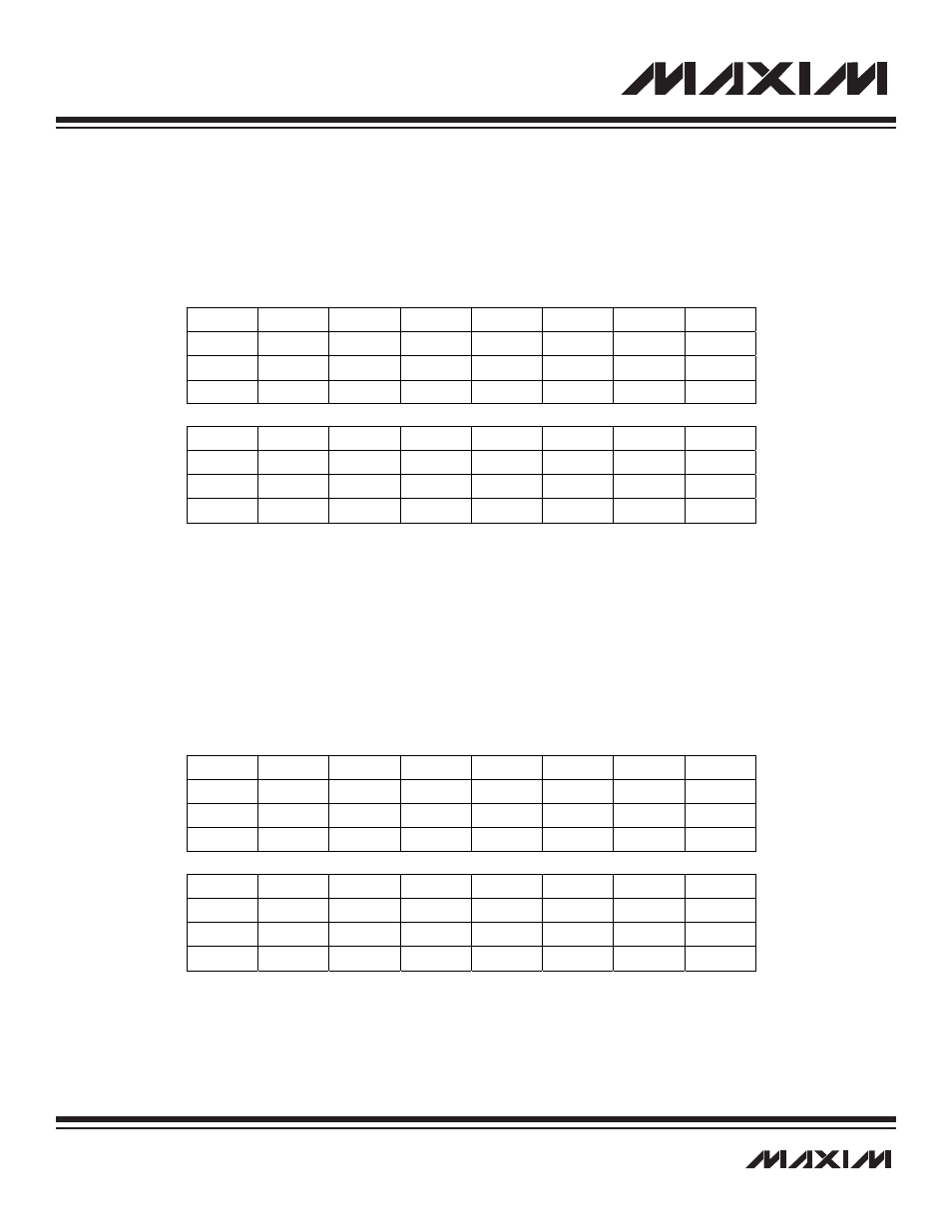
5.2.1 Port 0 Output Register (PO0)
Register Description:
Port 0 Output Register
Register Name:
PO0
Register Address:
Module 00h, Index 00h
Bits 15 to 8: Reserved. Read returns 0, write ignored.
Bits 7 to 0: Port 0 Output Register Bits 7:0 (PO0[7:0]). Port 0 is an enhanced Type D I/O port. The PO0 register stores output data
for port 0 when it is defined as an output port and controls whether the internal pullup resistor is enabled/disabled if a port pin is defined
as an input. The contents of this register can be modified by a write access. Reading from the register returns the contents of the reg-
ister. Changing the direction of port 0 does not change the data contents of the register.
5.2.2 Port 1 Output Register (PO1)
Register Description:
Port 1 Output Register
Register Name:
PO1
Register Address:
Module 00h, Index 01h
Bits 15 to 8: Reserved. Read returns 0, write ignored.
Bits 7 to 0: Port 1 Output Register Bits 7:0 (PO1[7:0]). Port 1 is an enhanced Type D I/O port. The PO1 register stores output data
for port 1 when it is defined as an output port and controls whether the internal weak pullup resistor is enabled/disabled if a port pin
is defined as an input. The contents of this register can be modified by a write access. Reading from the register returns the contents
of the register. Changing the direction of port 1 does not change the data contents of the register.
r = read, w = write
Note: This register is cleared to FFh on all forms of reset.
r = read, w = write
Note: This register is cleared to FFh on all forms of reset.
Bit #
15
14
13
12
11
10
9
8
Name
—
—
—
—
—
—
—
—
Reset
0
0
0
0
0
0
0
0
Access
r
r
r
r
r
r
r
r
Bit #
7
6
5
4
3
2
1
0
Name
PO07
PO06
PO05
PO04
PO03
PO02
PO01
PO00
Reset
1
1
1
1
1
1
1
1
Access
rw
rw
rw
rw
rw
rw
rw
rw
Bit #
15
14
13
12
11
10
9
8
Name
—
—
—
—
—
—
—
—
Reset
0
0
0
0
0
0
0
0
Access
r
r
r
r
r
r
r
r
Bit #
7
6
5
4
3
2
1
0
Name
PO17
PO16
PO15
PO14
PO13
PO12
PO11
PO10
Reset
1
1
0
0
0
0
0
0
Access
rw
rw
rw
rw
rw
rw
rw
rw
