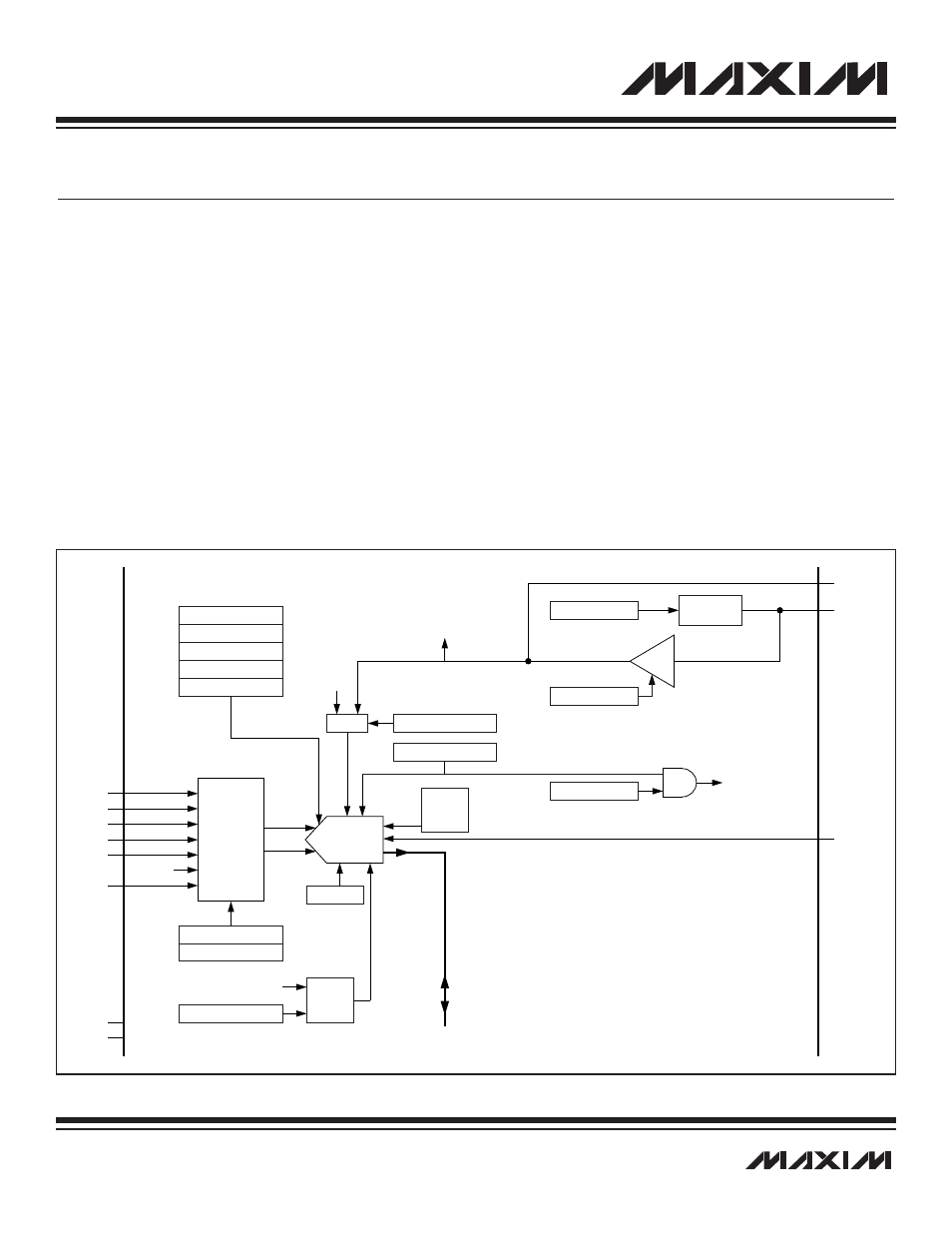
1 architecture, 1 architecture -3, Figure 14-1. sar adc block diagram -3 – Maxim Integrated MAXQ7667 User Manual
Page 235: Maxq7667 user’s guide

14-3
__________________________________________________________________________________________________________
MAXQ7667 User’s Guide
SECTION 14: SAR ADC MODULE
The MAXQ7667 incorporates a 12-bit SAR ADC with built-in sample-and-hold and a conversion rate up to 125ksps. The ADC allows gen-
eral-purpose measurements for temperature, supply voltage, diagnostics, or other parameters. Some of the features include the following:
•
Low-power, 125ksps, SAR (successive approximation) ADC, available as 12 bits.
•
ADC can measure up to five external, single-ended signals or two differential signals.
•
ADC has unipolar and bipolar modes with respective input ranges 0V to REF and -REF/2 to REF/2 (where REF is the reference
voltage).
•
An internal 2.5V bandgap-based voltage reference.
•
An external voltage reference between 1V and AVDD.
•
ADC can be used to measure the analog supply voltage, AVDD, without external connections.
•
ADC can use AVDD as its reference voltage, allowing ratiometric measurements proportional to the AVDD,
•
Selectable ADC conversion start source from on-chip timers, ADC conversion pin, and software write.
14.1 Architecture
Figure 14-1 shows the SAR ADC block diagram. The analog module is composed of a 12-bit SAR ADC and voltage reference blocks.
The input to the SAR ADC is fed through a multiplexer section. The input to the multiplexer can be set through software to measure five
single-ended or two differential inputs. The ADC can be configured to be in unipolar mode or bipolar mode.
Figure 14-1. SAR ADC Block Diagram
SARC[2:0]:SARS[2:0]
SARC[11:9]:SARMX[2:0]
REFERENCE TO
SIGMA-DELTA ADC
(SECTION 17)
ADC DATA
READY INTERRUPT
ASR.0:SARRDY
APE.12:BGE
APE.14:RBUFE
AIE.0:SARIE
BANDGAP
REF
SARC.3:SARBY
SARC.6:SARDUL
SARC.4:SARASD
SARC.7:SARBIP
SARC.8:SARDIF
OSCC[3:2]:SARCD[1:0]
ADC
CLOCK
DIV
TIMER 0
TIMER 1
TIMER 2
APE.4:SARE
ADCCLK
AVDD
V
REF
MUX
SARC[11:9]:SARMX[2:0]
12-BIT
ADC
AIN0
MUX
AIN1
AIN2
AIN3
DATA BUS[15:0]
AIN4
V
REF
AGND
AVDD
AGND
REFBG
ADCCTL
REF
SYSCLK
BUF
x1.0
