1 architecture, 2 uart/lin pins, 1 architecture -4 – Maxim Integrated MAXQ7667 User Manual
Page 134: 2 uart/lin pins -4, Figure 8-1. uart/lin block diagram -4, Table 8-1. gpio port 0 uart/lin pins -4, Maxq7667 user’s guide, Table 8-1. gpio port 0 uart/lin pins

___________________________________________________________________________________________________________
8-4
MAXQ7667 User’s Guide
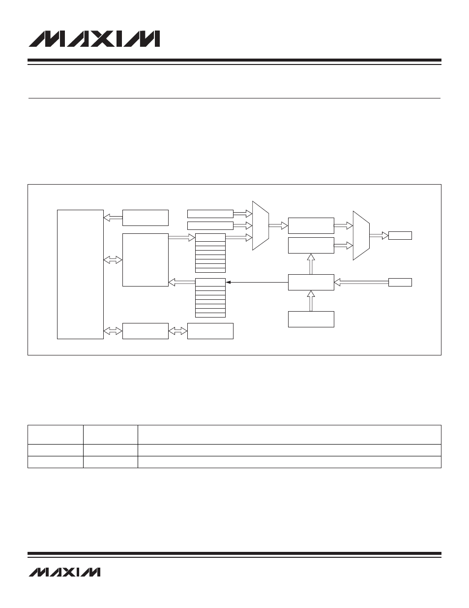
Figure 8-1. UART/LIN Block Diagram
MAXQ
CORE
INTERRUPTS
SBUF
REGISTER
TRANSMIT REGISTER
BREAK/SYNC
GENERATOR
LIN PROTOCOL
STATE MACHINES
LIN CONTROL
REGISTERS
CHECKSUM
PARITY
Tx FIFO
FILTER/RECEIVE
REGISTER
BAUD-RATE
GENERATOR
Tx PIN
Rx PIN
Rx FIFO
SECTION 8: UART AND LIN
The MAXQ7667 contains a standard UART for serial communication and dedicated hardware for support of the LIN bus. The dedicat-
ed LIN hardware simplifies the application code and requires less processor intervention. The MAXQ7667 can be configured to use
either the UART or LIN. Both the UART and LIN require external bus transceivers to connect to the physical layer.
8.1 Architecture
Figure 8-1 shows the various blocks that comprise the UART/LIN interface. The interface to the UART/LIN hardware is accessed
through the MAXQ7667 core. The MAXQ7667 memory-mapped registers for the UART/LIN are found in Module 3 of the peripheral reg-
ister map.
8.2 UART/LIN Pins
The UART/LIN pins are multiplexed with GPIO port 0 pins.
Table 8-1. GPIO Port 0 UART/LIN Pins
PORT P0
SIGNALS
PORT 0 PIN
FUNCTION
P0.0/URX
9
Port 0, Bit 0, General-Purpose Digital I/O Bit. Alternately, it is used for UART/LIN receive data.
P0.1/UTX
10
Port 0, Bit 1, General-Purpose Digital I/O Bit. Alternately, it is used for UART/LIN transmit data.
