3 uart and lin register de, 1 control register 1 (ua, 2 serial control registe – Maxim Integrated MAXQ7667 User Manual
Page 135: 3 uart and lin register descriptions -5, 1 control register 1 (uart) (cnt1) -5, 2 serial control register (uart) (scon) -5, Maxq7667 user’s guide, 3 uart and lin register descriptions, 1 control register 1 (uart) (cnt1), 2 serial control register (uart) (scon)

8-5
___________________________________________________________________________________________________________
MAXQ7667 User’s Guide
8.3 UART and LIN Register Descriptions
The following sections describe the MAXQ7667 registers that control the UART and LIN hardware.
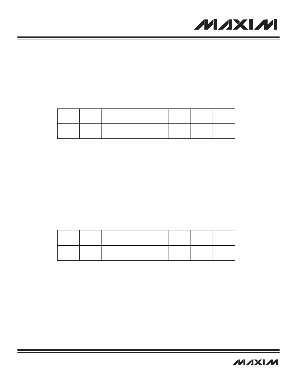
8.3.1 Control Register 1 (UART) (CNT1)
Attention: All the bits in this register should be written simultaneously in one write instruction.
Register Description:
Control Register 1 (UART)
Register Name:
CNT1
Register Address:
Module 03h, Index 05h
Bit 7: Receive or Transmit Mode (RTN). When a valid LIN header is received, the host must set this field to indicate whether the
peripheral should transmit (RTN = 0) or receive (RTN = 1) a LIN frame.
Bit 6: Checksum Type (CK). If the AUT bit (CNT0.3) is set to 1, this bit is set by the peripheral according to the checksum type for the
most recent frame. If AUT is cleared to 0, the MAXQ7667 must set this flag to indicate the checksum type to be used.
Bits 5 to 0: Frame Length (FL[5:0]). This field indicates the number of bytes in the frame. The frame length is always one greater than
the value specified in this field. For example, writing FL = 00h indicates a frame length of one byte and writing FL = 3Fh indicates a
frame length of 64 bytes.
8.3.2 Serial Control Register (UART) (SCON)
Register Description:
Serial Control Register (UART)
Register Name:
SCON
Register Address:
Module 03h, Index 06h
Bit 7: Serial Port Mode Bit 0/Framing Error Flag (SM0/FE). When the FEDE bit (SMD.0) is cleared to 0, this bit reflects the state of
the SM0 mode control bit. The host can write to this bit to configure the operating mode for legacy UART. When FEDE is set to 1, this
bit reflects the state of the framing error flag. The host can read this bit to determine the framing error status and can write this bit to
set or clear the framing error status. The serial port operating mode is defined in Table 8-2.
When the peripheral is configured for LIN master or LIN slave mode, the UART is always operated in mode 1 and the SM0 bit serves
no purpose. The FE flag reflects the framing error status in all LIN and UART modes.
Bit 6: Serial Port 0 Mode Bit 1 (SM1). If the peripheral is operating in legacy UART mode, this bit is the second mode control bit as
defined in Table 8-2.
r = read, w = write
Note: CNT1 is cleared to 80h on all forms of reset. The host must always write to this register after a valid identifier has been received.
Bit #
7
6
5
4
3
2
1
0
Name
RTN
CK
FL5
FL4
FL3
FL2
FL1
FL0
Reset
1
0
0
0
0
0
0
0
Access
rw
rw
rw
rw
rw
rw
rw
rw
r = read, w = write
Note: SCON is cleared to 00h on all forms of reset.
Bit #
7
6
5
4
3
2
1
0
Name
SM0/FE
SM1
SM2
REN
TB8
RB8
TI
RI
Reset
0
0
0
0
0
0
0
0
Access
rw
rw
rw
rw
rw
rw
rw
rw
