14 analog power enable, 14 analog power enable register (ape) -16, Maxq7667 user’s guide – Maxim Integrated MAXQ7667 User Manual
Page 298: 14 analog power enable register (ape)
17.3.14 Analog Power Enable Register (APE)
Register Description:
Analog Power Enable Register
Register Name:
APE
Register Address:
Module 05h, Index 10h
Bits 15 and 13: Reserved. Read returns 0.
Bit 14: Reference Buffer Enable (RBUFE). The reference buffer is enabled when set to 1 and disabled when set to 0.
Bit 12: Bandgap Enable (BGE). The reference buffer is enabled when set to 1 and disabled when set to 0.
Bit 11: I/O Linear Regulator Power-Down (LRIOPD). See Section 16 for details on this bit.
Bit 10: Digital Linear Regulator Power-Down (LRDPD). See Section 16 for details on this bit.
Bit 9: Analog Linear Regulator Power-Down (LRAPD). See Section 16 for details on this bit.
Bit 8: I/O Voltage Brownout Detection Enable (VIBE). See Section 16 for details on this bit.
Bit 7: Digital Voltage Reset Enable (VDPE). See Section 16 for details on this bit.
Bit 6: Digital Voltage Brownout Detection Enable (VDBE). See Section 16 for details on this bit.
Bit 5: Analog Voltage Brownout Detection Enable (VABE). See Section 16 for details on this bit.
Bit 4: SAR Enable (SARE). See Section 14 for details on this bit.
Bit 3: PLL Enable (PLLE). When set to 1, this bit enables PLL. When set to 0, this bit disables PLL and places it in a leakage-only
state.
Bit 2: Sigma-Delta Modulator Enable (MDE). When set to 1, this bit enables the sigma-delta modulator. When set to 0, this bit dis-
ables the modulator and places it in a leakage-only state.
Bit 1: LNA Enable (LNAE). When set to 1, this bit enables LNA. When set to 0, this bit disables LNA and places it in a leakage-only
state.
Bit 0: Bias Enable (BIASE). When set to 1, this bit enables the current bias generator. When set to 0, this bit disables the current bias
generator and places it in a leakage-only state. BIASE is automatically set to 1 whenever LNAE, MDE, PLLE, SARE, BGE or RBUFE is
set to 1.
_________________________________________________________________________________________________________
17-16
MAXQ7667 User’s Guide
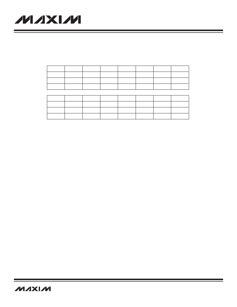
r = read, w = write
Note: APE is cleared to 0080h on all forms of reset.
Bit #
15
14
13
12
11
10
9
8
Name
—
RBUFE
—
BGE
LRIOPD
LRDPD
LRAPD
VIBE
Reset
0
0
0
0
0
0
0
0
Access
r
rw
r
rw
rw
rw
rw
rw
Bit #
7
6
5
4
3
2
1
0
Name
VDPE
VDBE
VABE
SARE
PLLE
MDE
LNAE
BIASE
Reset
1
0
0
0
0
0
0
0
Access
rw
rw
rw
r
rw
rw
rw
rw