13 pad drive strength re, 14 pad drive strength re, 15 pad resistive pull di – Maxim Integrated MAXQ7667 User Manual
Page 89: 13 pad drive strength register (port 0) (ps0) -14, 14 pad drive strength register (port 1) (ps1) -14, Maxq7667 user’s guide, 13 pad drive strength register (port 0) (ps0), 14 pad drive strength register (port 1) (ps1)
__________________________________________________________________________________________________________
5-14
MAXQ7667 User’s Guide
In addition to the standard enhanced Type D GPIO port features, the MAXQ7667 offers programmable drive strength and program-
mable direction of resistive pullup or pulldown.
5.2.13 Pad Drive Strength Register (Port 0) (PS0)
Register Description:
Pad Drive Strength Register (Port 0)
Register Name:
PS0
Register Address:
Module 00h, Index 18h
Bits 7 to 0: Port 0 Drive Strength Register Bits 7:0 (PS0[7:0]). When the port direction register PD0 configures a particular I/O pin
as an output, the corresponding PS0 bit configures the drive strength of that output. When a PS0 bit is set to 0, the output driver is 1mA
(typical). When set to 1 the output driver is 2mA (typical).
5.2.14 Pad Drive Strength Register (Port 1) (PS1)
Register Description:
Pad Drive Strength Register (Port 1)
Register Name:
PS1
Register Address:
Module 00h, Index 19h
Bits 7 to 0: Port 1 Drive Strength Register Bits 7:0 (PS1[7:0]). When the port direction register PD1 configures a particular I/O pin
as an output, the corresponding PS1 bit configures the drive strength of that output. When a PS0 bit is set to 0, the output driver is 1mA
(typical). When set to 1 the output driver is 2mA (typical).
5.2.15 Pad Resistive Pull Direction Register (Port 0) (PR0)
Register Description:
Pad Resistive Pull Direction Register (Port 0)
Register Name:
PR0
Register Address:
Module 00h, Index 1Bh
Bits 7 to 0: Port 0 Resistive Select Bits 7:0 (PR0[7:0]). When the port direction register PD0 configures a particular I/O pin as an
input, and the corresponding PO0 register bit enables a resistive pull, PR0 controls the direction of that pull. If the PR0 bit is set to 0,
the I/O pin has a resistive pulldown of approximately 150k
Ω (typical). When the PR0 bit is set to 1, the I/O pin has a resistive pullup of
approximately 150k
Ω (typical).
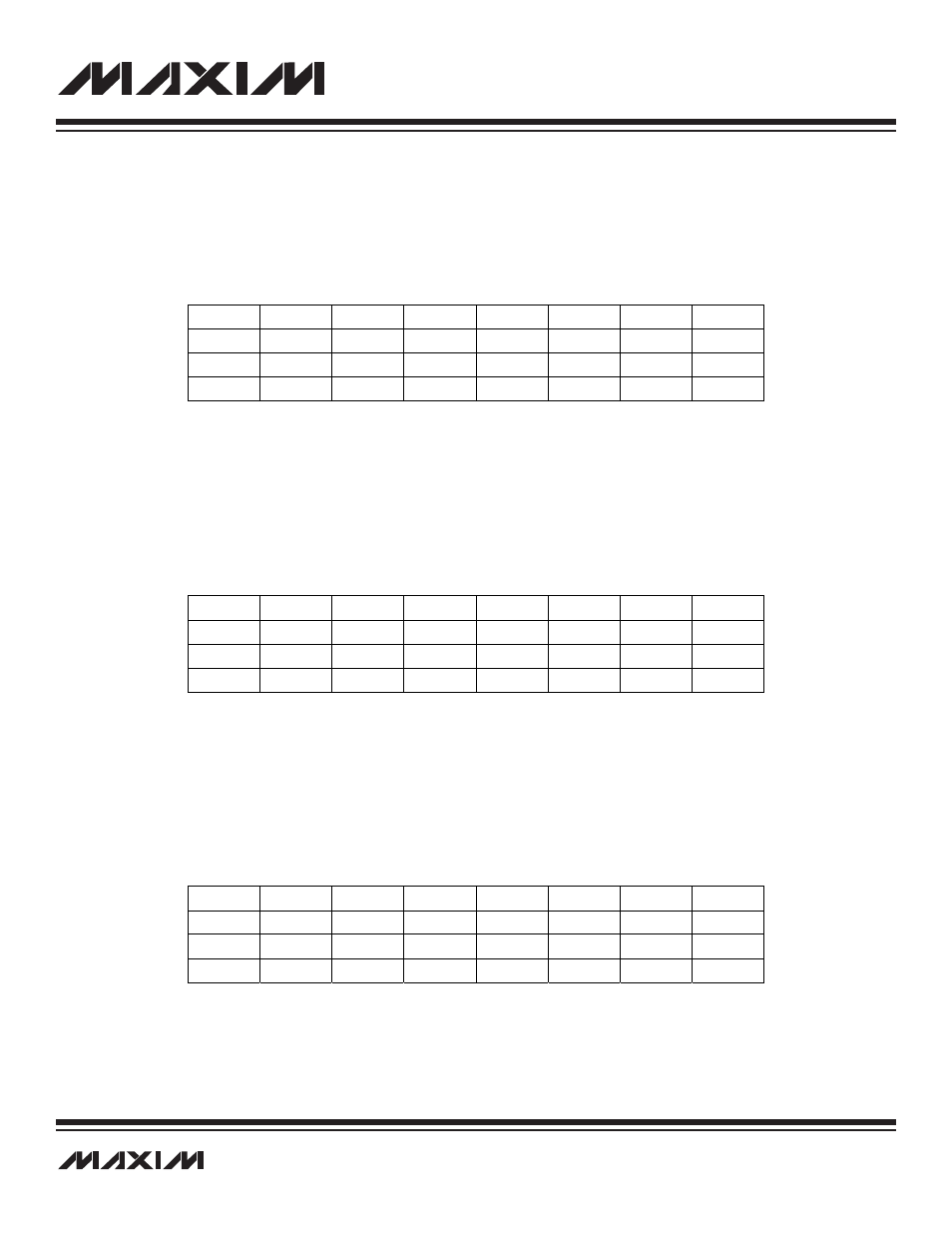
r = read, w = write
Note: This register is cleared to 00h on all forms of reset.
Bit #
7
6
5
4
3
2
1
0
Name
PS07
PS06
PS05
PS04
PS03
PS02
PS01
PS00
Reset
0
0
0
0
0
0
0
0
Access
rw
rw
rw
rw
rw
rw
rw
rw
r = read, w = write
Note: This register is cleared to 00h on all forms of reset.
Bit #
7
6
5
4
3
2
1
0
Name
PS17
PS16
PS15
PS14
PS13
PS12
PS11
PS10
Reset
0
0
0
0
0
0
0
0
Access
rw
rw
rw
rw
rw
rw
rw
rw
r = read, w = write
Note: This register is cleared to FFh on all forms of reset.
Bit #
7
6
5
4
3
2
1
0
Name
PR07
PR06
PR05
PR04
PR03
PR02
PR01
PR00
Reset
1
1
1
1
1
1
1
1
Access
rw
rw
rw
rw
rw
rw
rw
rw