4 spi clock register, 4 spi clock register (spick) -10, Maxq7667 user’s guide – Maxim Integrated MAXQ7667 User Manual
Page 172

__________________________________________________________________________________________________________
9-10
MAXQ7667 User’s Guide
Bit 1: Clock Phase Select (CKPHA). This bit selects the clock phase and is used with the CKPOL bit to define the SPI data transfer
format.
0 = Data sampled on the active clock edge.
1 = Data sampled on the inactive clock edge.
Bit 0: Clock Polarity Select (CKPOL). This bit selects the clock polarity and is used with the CKPHA bit to define the SPI data trans-
fer format.
0 = Clock idles in the logic 0 state (rising = active clock edge).
1 = Clock idles in the logic 1 state (falling = active clock edge).
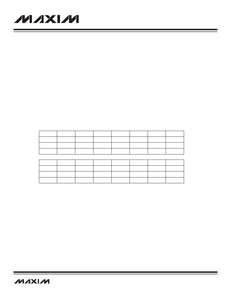
9.1.1.4 SPI Clock Register (SPICK)
The SPI clock register (SPICK) contains the divider ratio from the system clock to set the SPI port baud rate. In master mode, the max-
imum clock frequency allowed is one-half the system clock rate. The SPI baud rate is selected by:
SPI master baud rate = (0.5 x system clock frequency)/(SPICK[7:0]) +1
In slave mode, the SPI clock is an input driven by an external master device. That rate is limited to a maximum of one-eighth the sys-
tem clock.
Register Description:
SPI Clock Register
Register Name:
SPICK
Register Address:
Module 01h, Index 09h
Bits 15 to 8: Reserved. Read 0, write ignored.
Bits 7 to 0: SPI Clock Divider Ratio (SPICK[7:0]). This value is a number that ranges from 0 to 255.
Bit #
15
14
13
12
11
10
9
8
Name
—
—
—
—
—
—
—
—
Reset
0
0
0
0
0
0
0
0
Access
r
r
r
r
r
r
r
r
Bit #
7
6
5
4
3
2
1
0
Name
SPICK7
SPICK6
SPICK5
SPICK4
SPICK3
SPICK2
SPICK1
SPICK0
Reset
0
0
0
0
0
0
0
0
Access
rw
rw
rw
rw
rw
rw
rw
rw
r = read, w = write
