3 tap interface control, 1 system control regist, 3 tap interface control -4 – Maxim Integrated MAXQ7667 User Manual
Page 193: 1 system control register (sc) -4, Maxq7667 user’s guide, 1 system control register (sc)

__________________________________________________________________________________________________________
11-4
MAXQ7667 User’s Guide
11.3 TAP Interface Control
Once an application has been loaded and starts running, the MAXQ7667 JTAG TAP interface can be controlled by the TAP bit in the
system control register as described in Section 11.3.1.
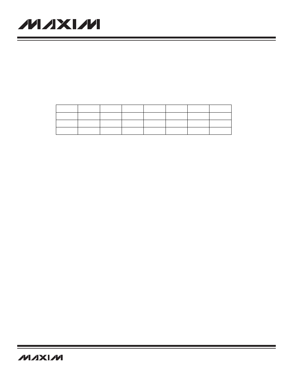
11.3.1 System Control Register (SC)
Register Description:
System Control Register
Register Name:
SC
Register Address:
Module 08h, Index 08h
Bit 7: Test Access (JTAG) Port Enable (TAP). This bit controls whether the TAP special function pins are enabled. The TAP defaults
to being enabled.
0 = JTAG/TAP functions are disabled and P1.0–P1.3 can be used as general-purpose I/O pins
1 = TAP special function pins P1.0–P1.3 are enabled to act as JTAG inputs and outputs
Bits 6 and 0: Reserved.
Bits 5 and 4: Code Data Access Bits 1 and 0 (CDA[1:0]). See Section 4 for more information on these bits.
Bit 3: Upper Program Access (UPA). See Section 2 for more information on this bit.
Bit 2: ROM Operation Done (ROD). See Section 12 for more information on this bit.
Bit 1: Password Lock (PWL). See Section 12 for more information on this bit.
Bit #
7
6
5
4
3
2
1
0
Name
TAP
—
CDA1
CDA0
UPA
ROD
PWL
—
Reset
0
0
0
0
0
0
1
0
Access
rw
r
rw
rw
rw
rw
rw
r
r = read, w = write
*This register defaults to 80h on all forms of reset except after power-on reset. After power-on reset, the PWL bit is also set and this register defaults to 82h.
