3 echo path control reg, 3 echo path control register (rcvc) -8, Maxq7667 user’s guide – Maxim Integrated MAXQ7667 User Manual
Page 290: 3 echo path control register (rcvc)

Bit 11: Burst Polarity Control (BPOL). Setting this bit to 0 causes a low idle state and a high pulse width of BPH. Set BPOL 1 to invert
the BURST output, idling high with BPH specifying the low period within the period.
Bit 10: Burst Clock Source Select (BCKS). Setting this bit to 0 selects the PLL output as the clock source for burst transmission and
for the echo receive path. Setting this bit to 1 selects the system clock as the clock source for burst transmission and for the echo
receive path. The reset state sets this bit to a 1, selecting the system clock.
Bit 9: Burst Three-State (BTRI). When set to 1, this bit places the burst output pad in a high-impedance state to allow internal trans-
mit/receive path testing.
Bit 8: Burst Gate (BGT). When set to 1, this bit immediately gates the output of the burst pulse, driving the ouput to its nonasserted
state (dependent on the polarity selection BPOL).
Bits 7 to 0: Burst Pulse Count (BCNT[7:0]). Defines the number of burst pulses (at least 1) transmitted each time BSTT is set to 1.
When BCNT is 0, there is still one pulse to be transmitted.
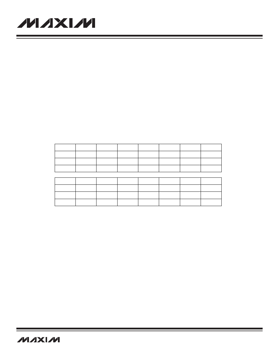
17.3.3 Echo Path Control Register (RCVC)
Register Description:
Echo Path Control Register
Register Name:
RCVC
Register Address:
Module 05h, Index 03h
Bits 15 to 9 and 5: Reserved. Read returns 0.
Bits 8: LNA Output Mux Select (LNAOSEL). When set to 1, this bit routes LNA outputs to AIN0 and AIN1.
Bits 7 and 6: LNA Input Mux Select (LNAISEL[1:0]). Determines LNA input connections.
00 selects ECHOP and ECHON
01 selects AGND vs. AGND
10 selects 2mV
P-P
vs. AGND
11 is reserved
Bits 4 to 0: Echo Receive Path Gain Control (RCVGN[4:0])
00000 selects gain of 32dB
11111 selects gain of 50dB
__________________________________________________________________________________________________________
17-8
MAXQ7667 User’s Guide
r = read, w = write
Note: RCVC is cleared to 0000h on all forms of reset.
Bit #
15
14
13
12
11
10
9
8
Name
—
—
—
—
—
—
—
LNAOSEL
Reset
0
0
0
0
0
0
0
0
Access
r
r
r
r
r
r
r
rw
Bit #
7
6
5
4
3
2
1
0
Name
LNAISEL1
LNAISEL0
—
RCVGN4
RCVGN3
RCVGN2
RCVGN1
RCVGN0
Reset
0
0
0
0
0
0
0
0
Access
rw
rw
r
rw
rw
rw
rw
rw
