Table 12-2. background mode debug commands -16, Maxq7667 user’s guide, Table 12-2. background mode debug commands – Maxim Integrated MAXQ7667 User Manual
Page 214
_________________________________________________________________________________________________________
12-16
MAXQ7667 User’s Guide
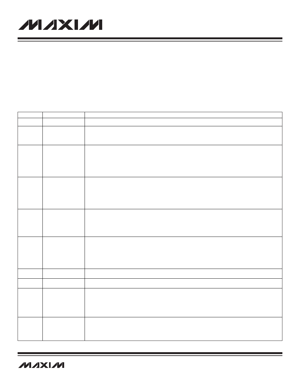
Table 12-2. Background Mode Debug Commands
OP CODE
COMMAND
OPERATION
0010-0000
No Operation
No Operation
0010-0001
Read Register Map
Read Data from Internal Registers. This command forces the debug engine to update the CMD[3:0] bits in the
ICDC to 0001b and perform a jump to ROM code at 8010h. The ROM debug service routine will load register data to
ICDB for host capture/read, starting at the lowest register location in module 0, one byte at a time in a successive
order until all internal registers are read and output to the host.
0010-0010
Read Data Memory
Read Data from Data Memory. This command requires four follow-on transfer cycles, two for the starting address
and two for the word read count, starting with the LSB address and ending with the MSB read count. The address is
moved to the ICDA register and the word read count is moved to the ICDD register by the debug engine. This
information is directly accessible by the ROM code. At the completion of this command period, the debug engine
updates the CMD[3:0] bits to 0010b and performs a jump to ROM code at 8010h. The ROM debug service routine
will load ICDB from data memory according to address and count information provided by the host.
0010-0011
Read Program Stack
Read Data from Program Stack. This command requires four follow-on transfer cycles, two for the starting address
and two for the read count, starting with the LSB address and ending with the MSB read count. The address is
moved to the ICDA register and the read count is moved to the ICDD register by the debug engine. This information
is directly accessible by the ROM code. At the completion of this command period, the debug engine updates the
CMD[3:0] bits to 0011b and performs a jump to ROM code at 8010h. The ROM Debug service routine will pop data
out from the stack according to the information received in the ICDA and ICDD register. The stack pointer is pre-
decremented for each pop operation.
0010-0100
Write Register
Write Data to a Selected Register. This command requires four follow-on transfer cycles, two for the register
address and two for the data, starting with the LSB address and ending with the MSB data. The address is moved to
the ICDA register and the data is moved to the ICDD register by the debug engine. This information
is directly accessible by the ROM code. At the completion of this command period, the debug engine updates the
CMD[3:0] bits to 0100b and performs a jump to ROM code at 8010h. The ROM Debug service routine will update
the select register according to the information received in the ICDA and ICDD registers.
0010-0101
Write Data Memory
Write Data to a Selected Data Memory Location. This command requires four follow-on transfer cycles, two for
the memory address and two for the data, starting with the LSB address and ending with the MSB data. The address
is moved to the ICDA register and the data is moved to the ICDD register by the debug engine. This information is
directly accessible by the ROM code. At the completion of this command period, the debug engine updates the
CMD[3:0] bits to 0101b and performs a jump to ROM code at 8010h. The ROM Debug service routine will update
the selected data memory location according to the information received in the |CDA and ICDD registers.
0010-0110
Trace
Trace Command. This command allows single stepping the CPU and requires no follow-on transfer cycle. The
trace operation is a ‘debug mode exit, one cycle CPU execution, debug mode entry’ sequence.
0010-0111
Return
Return Command. This command terminates the debug mode and returns the debug engine to background mode.
This allows the CPU to resume its normal operation at the point where it has been last interrupted.
0010-1000
Unlock Password
Unlock the Password Lock. This command requires 32 follow-on transfer cycles each containing a byte value
to be compared with the program memory password for the purpose of clearing the PWL bit and granting access to
protected debug and loader functions. When this command is received, the debug engine updates the CMD[3:0]
bits to 1000b and performs a jump to ROM code at 8010h. Data is loaded to the ICDB register when each byte of
data is received, beginning with the LSB of the least significant word first and end with the MSB of the most
significant word.
0010-1001
Read Register
Read from a Selected Internal Register. This command requires two follow-on transfer cycles, starting with the
LSB address and ending with the MSB address. The address is moved to ICDA register by the debug engine. This
information is directly accessible by the ROM code. At the completion of this command period, the debug engine
updates the CMD[3:0] bits to 1001b and performs a jump to ROM code at 8010h. The ROM Debug service routine
will always assume a 16-bit register length and return the requested data LSB first.
Internally, the ROM can ascertain when new data is available or when it can output the next data byte via the TXC flag. The TXC flag is an
important indicator between the debug engine and the utility ROM debug routines. The utility ROM firmware sets the TXC flag to 1 to indi-
cate that valid data has been loaded to the ICDB register. The debug engine clears the TXC flag to 0 to indicate completion of a data shift
cycle, thus allowing the ROM to continue execution of a requested task that is still in progress. The utility ROM signals that it has com-
pleted a requested task by setting the ROM operation done (ROD) bit of the SC register to logic 1. The ROD bit is reset by the debug
engine when it recognizes the done condition. Table 12-2 shows the debug mode commands supported by the MAXQ7667. Note that
background mode commands are supported inside debug mode. Encodings not listed in this table are not supported in debug mode and
are treated as no operations.