3 a20 gate, Figure 15.2 typical lframe timing – Renesas H8S/2111B User Manual
Page 432
Rev. 1.00, 05/04, page 398 of 544
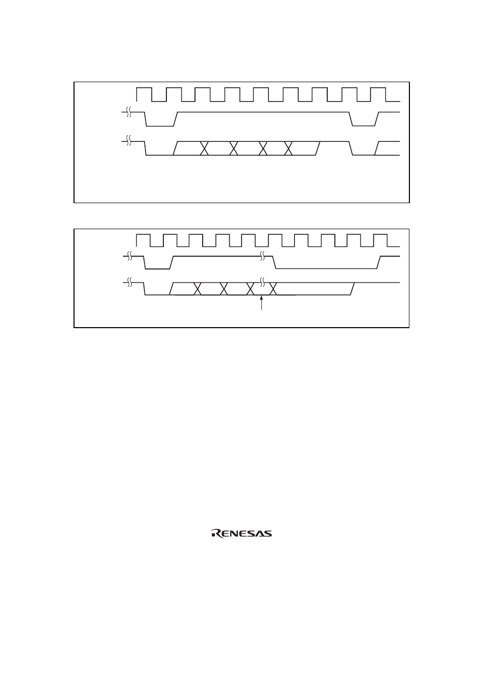
The timing of the
LFRAME, LCLK, and LAD signals is shown in figures 15.2 and 15.3.
ADDR
Start
LFRAME
LAD3–LAD0
Number of clocks
LCLK
TAR
Sync
Data
TAR
Start
Cycle type,
direction,
and size
1
1
4
1
2
2
2
1
Figure 15.2 Typical
LFRAME Timing
ADDR
Start
LFRAME
LAD3–LAD0
LCLK
TAR
Sync
Cycle type,
direction,
and size
Slave must stop driving
Too many Syncs
cause timeout
Master will
drive high
Figure 15.3 Abort Mechanism
15.4.3 A20
Gate
The A20 gate signal can mask address A20 to emulate an addressing mode used by personal
computers with an 8086*-family CPU. A regular-speed A20 gate signal can be output under
firmware control. The fast A20 gate function that is speeded up by hardware is enabled by setting
the FGA20E bit to 1 in HICR0.
Note: An Intel microprocessor