Renesas H8S/2111B User Manual
Page 158
Rev. 1.00, 05/04, page 124 of 544
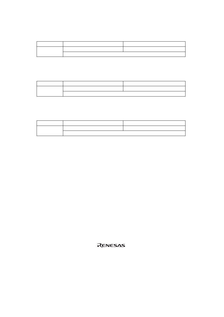
• P92/IRQ0
The pin function is switched as shown below according to the state of the P92DDR bit.
P92DDR 0
1
P92 input pin
P92 output pin
Pin Function
IRQ0 input pin*
Note: * When bit IRQ0E in IER is set to 1, this pin is used as the
IRQ0 input pin.
• P91/IRQ1
The pin function is switched as shown below according to the state of the P91DDR bit.
P91DDR 0
1
P91 input pin
P91 output pin
Pin Function
IRQ1 input pin*
Note: * When bit IRQ1E in IER is set to 1, this pin is used as the
IRQ1 input pin.
• P90/IRQ2/ADTRG
The pin function is switched as shown below according to the state of the P90DDR bit.
P90DDR 0
1
P90 input pin
P90 output pin
Pin Function
IRQ2 input pin, ADTRG input pin*
Note: * When the IRQ2E bit in IER is set to 1, this pin is used as the
IRQ2 input pin. When both
bits TRGS1 and TRGS0 in ADCR of the A/D converter are set to 1, this pin is used as
the
AGTRG input pin.