3 clock – Renesas H8S/2111B User Manual
Page 286
Rev. 1.00, 05/04, page 252 of 544
12.4.3 Clock
Either an internal clock generated by the on-chip baud rate generator or an external clock input at
the SCK pin can be selected as the SCI's transfer clock, according to the setting of the C/
A bit in
SMR and the CKE1 and CKE0 bits in SCR. When an external clock is input at the SCK pin, the
clock frequency should be 16 times the bit rate used.
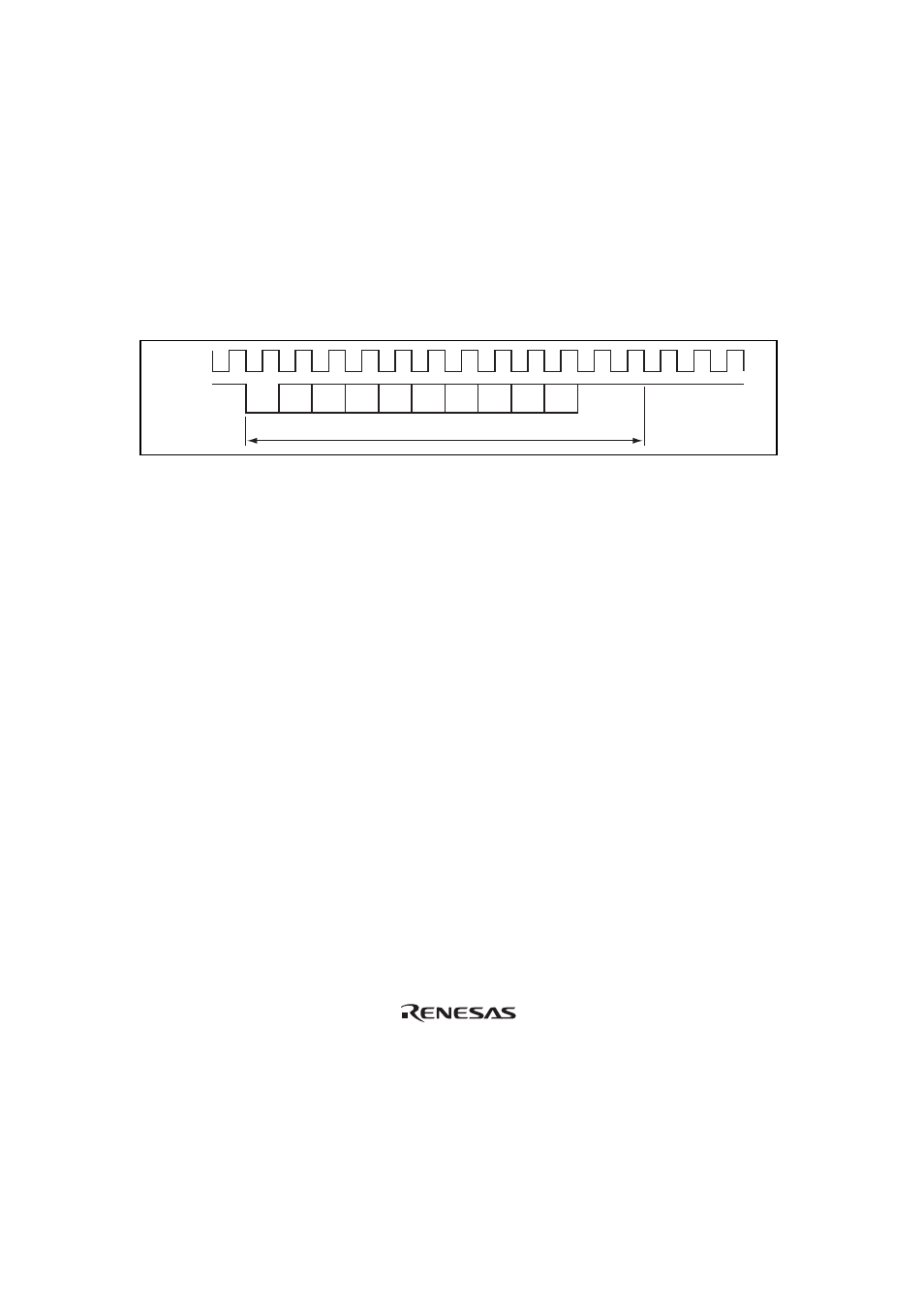
When the SCI is operated on an internal clock, the clock can be output from the SCK pin. The
frequency of the clock output in this case is equal to the bit rate, and the phase is such that the
rising edge of the clock is in the middle of the transmit data, as shown in figure 12.4.
0
1 frame
D0
D1
D2
D3
D4
D5
D6
D7
0/1
1
1
SCK
TxD
Figure 12.4 Relation between Output Clock and Transmit Data Phase
(Asynchronous Mode)