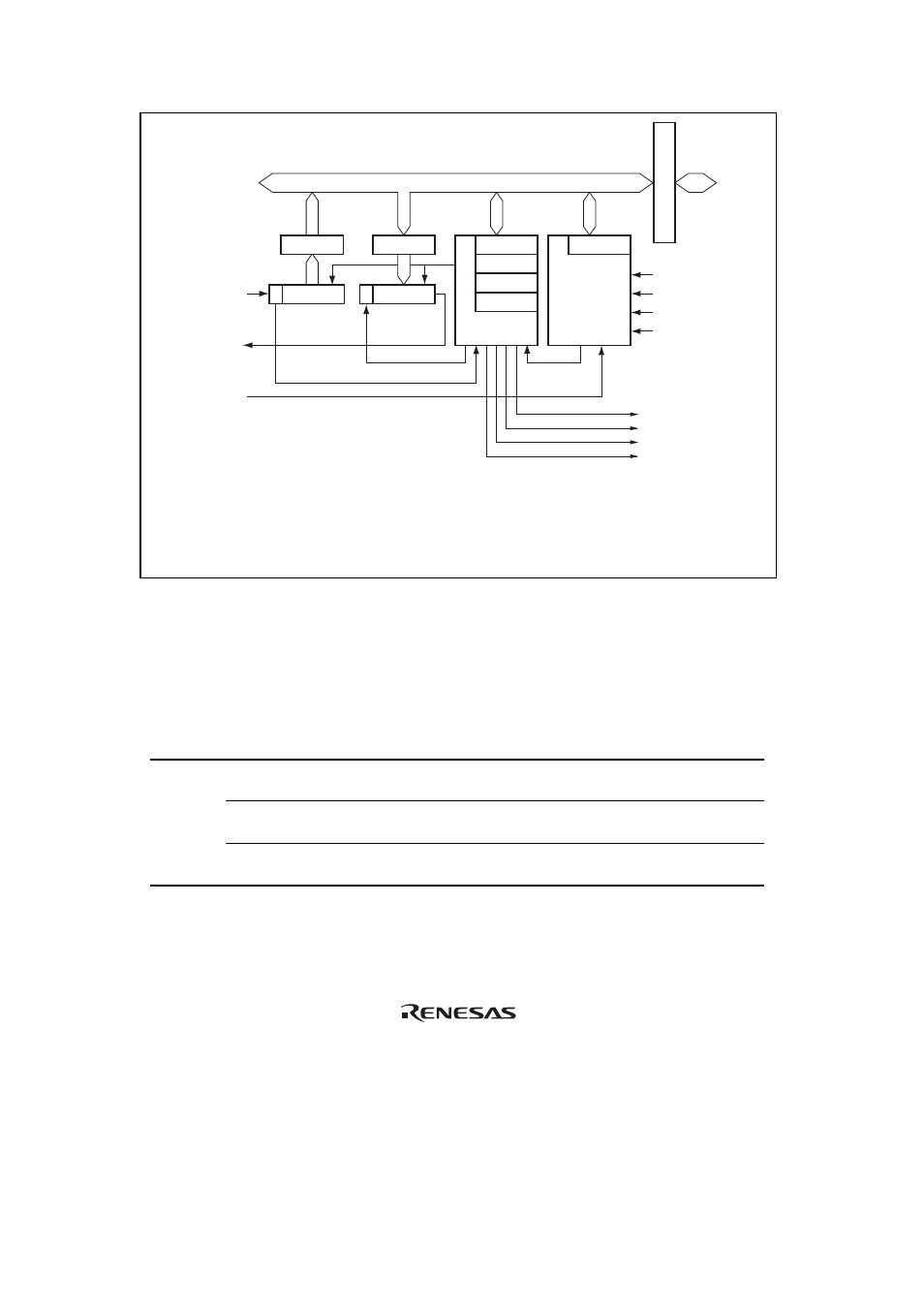
2 input/output pins, Figure 12.1 block diagram of sci – Renesas H8S/2111B User Manual
Page 270

Rev. 1.00, 05/04, page 236 of 544
ExRxD*/RxD
ExTxD*/TxD
ExSCK*/SCK
Clock
φ
φ/4
φ/16
φ/64
TEI
TXI
RXI
ERI
SCMR
SSR
SCR
SMR
Transmission/
reception control
Baud rate
generator
BRR
Module data bus
RDR
TSR
RSR
Parity generation
Parity check
[Legend]
RSR:
Receive shift register
RDR:
Receive data register
TSR:
Transmit shift register
TDR: Transmit
data
register
SMR:
Serial mode register
TDR
Bus interface
Internal data bus
External clock
SCR:
Serial control register
SSR:
Serial status register
SCMR: Smart card mode register
BRR:
Bit rate register
Note: * The program development tool (emulator) does not support this function.
Figure 12.1 Block Diagram of SCI
12.2 Input/Output
Pins
Table 12.1 shows the input/output pins for each SCI channel.
Table 12.1 Pin Configuration
Channel Symbol
*
1
Input/Output
Function
SCK1/
ExSCK1*
2
Input/Output Channel
1 clock input/output
RxD1/
ExRxD1*
2
Input
Channel 1 receive data input
1
TxD1/
ExTxD1*
2
Output
Channel 1 transmit data output
Notes: 1. Pin names SCK, RxD, and TxD are used in the text for all channels, omitting the
channel designation.
2. The program development tool (emulator) does not support this function.
