Section 8 8-bit pwm timer (pwm), 1 features, Figure 8.1 shows a block diagram of the pwm timer – Renesas H8S/2111B User Manual
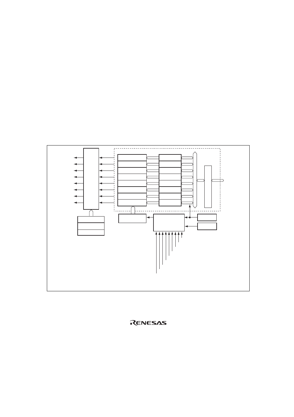
Page 181: Figure 8.1 block diagram of pwm timer
PWM0800B_000120040200
Rev. 1.00, 05/04, page 147 of 544
Section 8 8-Bit PWM Timer (PWM)
This LSI has an on-chip pulse width modulation (PWM) timer with eight outputs. Eight output
waveforms are generated from a common time base, enabling PWM output with a high carrier
frequency to be produced using pulse division. Connecting a low pass filter externally to the LSI
enables the PWM to function as an 8-bit D/A converter.
8.1 Features
• Operable at a maximum carrier frequency of 625 kHz using pulse division (at 10 MHz
operation)
• Duty cycles from 0 to 100% with 1/256 resolution (100% duty realized by port output)
• Direct or inverted PWM output, and PWM output enable/disable control
Figure 8.1 shows a block diagram of the PWM timer.
P10/PW0
P11/PW1
P12/PW2
P13/PW3
P14/PW4
P15/PW5
P16/PW6
P17/PW7
Comparator 0
Comparator 1
Comparator 2
Comparator 3
Comparator 4
Comparator 5
Comparator 6
Comparator 7
PWDR0
PWDR1
PWDR2
PWDR3
PWDR4
PWDR5
PWDR6
PWDR7
PWSL
PWDPRA
PWOERA
P1DDR
[Legend]
Note: * The program development tool (emulator) does not support this function.
PWSL:
PWDR:
PWDPRA:
PWOERA:
PCSR:
P1DDR:
PWM register select
PWM data register
PWM data polarity register A
PWM output enable register A
Peripheral clock select register
Port 1 data direction register
PCSR
Port/PWM output control
Module
data bus
Internal
data bus
Bus interface
Select
clock
Clock
counter
Internal clock
φ
φ/8
φ/2
φ/4
φ/16
φ/256*
φ/4096*
φ/512*
φ/1024*
Figure 8.1 Block Diagram of PWM Timer