5 port g nch-od control register (pgnocr), 6 pin functions – Renesas H8S/2111B User Manual
Page 179
Rev. 1.00, 05/04, page 145 of 544
• PG3, PG2, PG1, PG0
The pin function is switched as shown below according to the state of the PGnDDR bit.
PGnDDR 0
1
Pin Function
PGn input pin
PGn output pin
[Legend]
n
= 3 to 0
7.14.5 Port G Nch-OD Control Register (PGNOCR)
PGNOCR specifies the output driver type for pins on port G which are configured as outputs on a
bit-by-bit basis.
Bit Bit
Name
Initial
Value R/W Description
7 PG7NOCR 0 R/W
6 PG6NOCR 0 R/W
5 PG5NOCR 0 R/W
4 PG4NOCR 0 R/W
3 PG3NOCR 0 R/W
2 PG2NOCR 0 R/W
1 PG1NOCR 0 R/W
0 PG0NOCR 0 R/W
0: NMOS push-pull (Vcc-side n-channel driver enabled)
1: Vss-side N-channel open drain (Vcc-side N-channel
driver disabled)
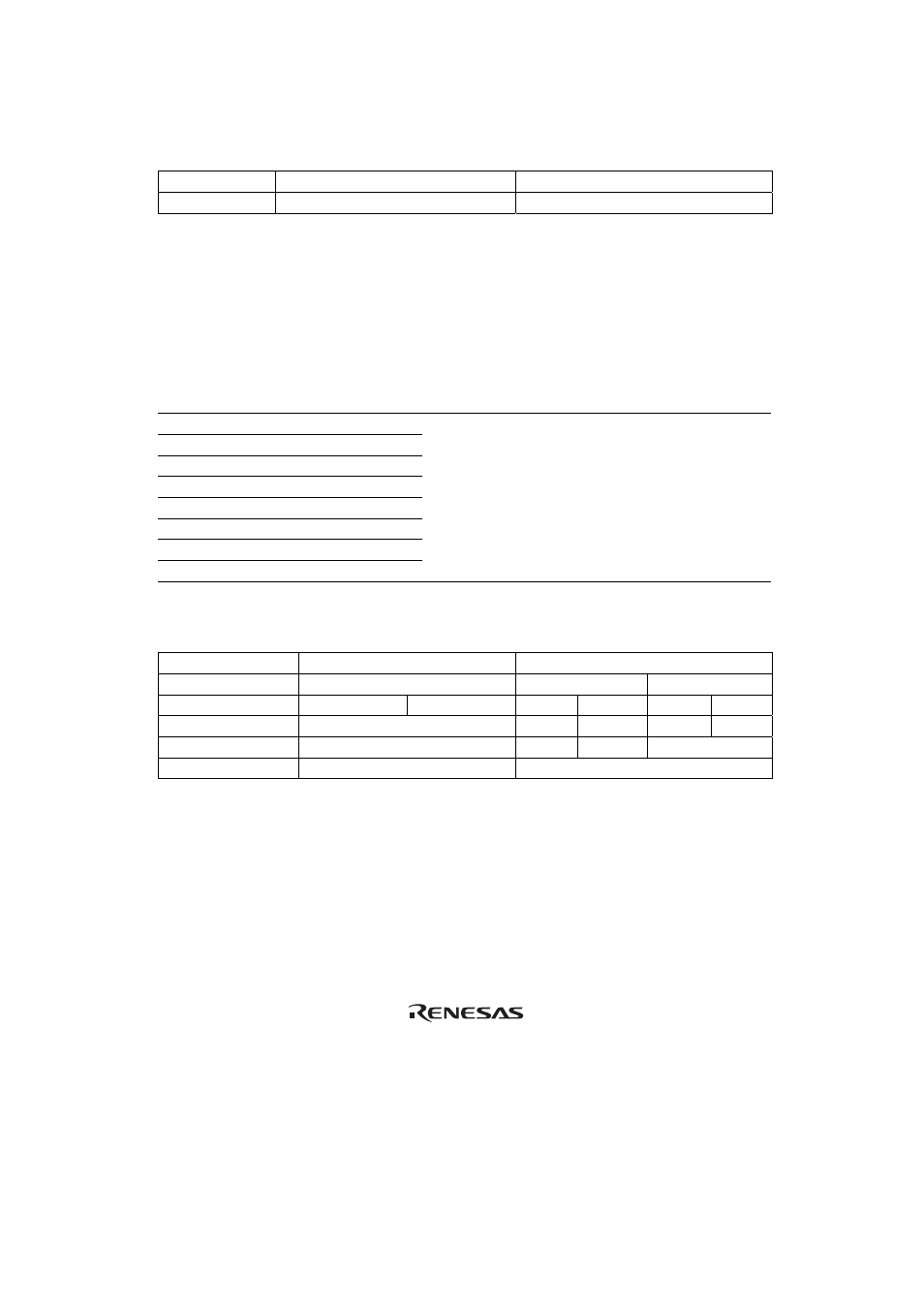
7.14.6 Pin
Functions
DDR 0
1
NOCR —
0
1
ODR 0
1
0
1
0
1
V
ss
-side N-ch. driver
OFF
ON
OFF
ON
OFF
V
cc
-side N-ch. driver
OFF
OFF
ON
OFF
Pin function
Input pin
Output pin*
Note: * Except when set as IIC I/O pin.