Renesas H8S/2111B User Manual
Page 309
Rev. 1.00, 05/04, page 275 of 544
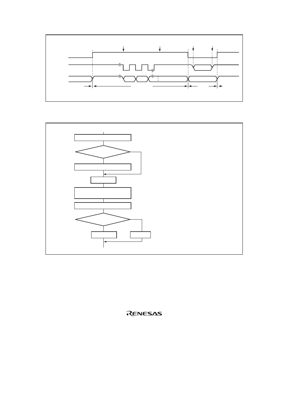
TE bit
SCK
output pin
TxD
output pin
Port input/output
Port
input/output
Port
input/output
High output*
Marking output
Transmission start
Transmission end
Transition to
software standby
mode
Software standby
mode cancelled
SCI TxD output
Port
Port
SCI
TxD output
Last TxD bit retained
Note: * Initialized in software standby mode
Figure 12.23 Pin States during Transmission in Clocked Synchronous Mode
(Internal Clock)
Start reception
Reception
[1]
No
No
Yes
Yes
Read receive data in RDR
Read RDRF flag in SSR
Make transition to software
standby mode etc.
Cancel software standby mode etc.
RE = 0
Initialization
RE = 1
[2]
Change operating mode?
RDRF = 1
[1] Data being received will be invalid.
[2] Module stop, watch, sub-active, and
sub-sleep modes are included
Figure 12.24 Sample Flowchart for Mode Transition during Reception