2 input/output pins – Renesas H8S/2111B User Manual
Page 384
Rev. 1.00, 05/04, page 350 of 544
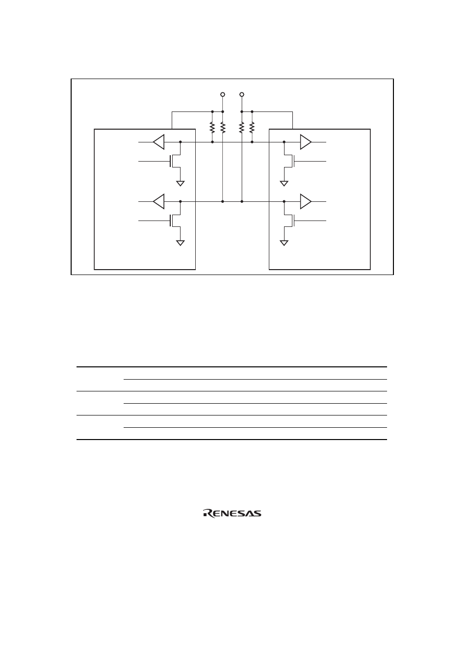
Figure 14.2 shows how the keyboard buffer controller is connected.
Vcc
KCLK in
KCLK out
KD in
KD out
Keyboard buffer controller
(This LSI)
System side
KCLK in
KCLK out
KD in
KD out
I/F
Keyboard side
Vcc
Clock
Data
Figure 14.2 Keyboard Buffer Controller Connection
14.2 Input/Output
Pins
Table 14.1 lists the input/output pins used by the keyboard buffer controller.
Table 14.1 Pin Configuration
Channel Name
Abbreviation
*
I/O Function
KBC clock I/O pin (KCLK0)
PS2AC
I/O
KBC clock input/output
0
KBC data I/O pin (KD0)
PS2AD
I/O
KBC data input/output
KBC clock I/O pin (KCLK1)
PS2BC
I/O
KBC clock input/output
1
KBC data I/O pin (KD1)
PS2BD
I/O
KBC data input/output
KBC clock I/O pin (KCLK2)
PS2CC
I/O
KBC clock input/output
2
KBC data I/O pin (KD2)
PS2CD
I/O
KBC data input/output
Note: * These are the external I/O pin names. In the text, clock I/O pins are referred to as KCLK
and data I/O pins as KD, omitting the channel designations.