3 pin functions – Renesas H8S/2111B User Manual
Page 153
Rev. 1.00, 05/04, page 119 of 544
7.8.3 Pin
Functions
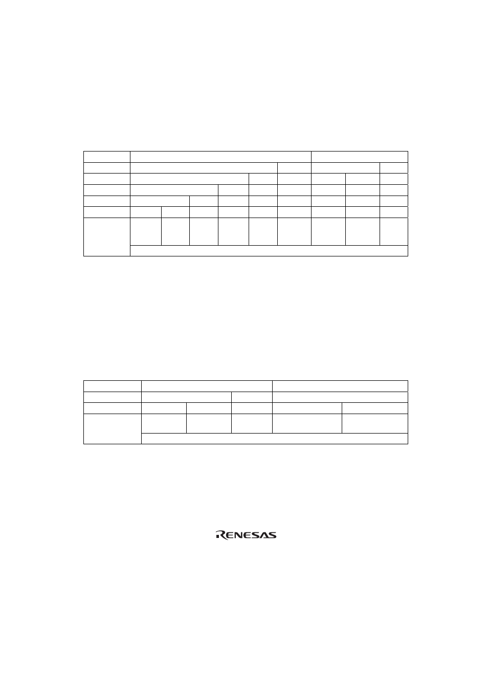
• P86/IRQ5/SCK1/SCL1
The pin function is switched as shown below according to the combination of the C/
A bit in
SMR of SCI_1, the CKE0 and CKE1 bits in SCR, the SPS1 bit*
2
in SPSR, the ICE bit in ICCR
of IIC_1, the IIC1AS and the IIC1BS bits in PGCTL*
3
, and the 86DDR bit.
P86ICE
= ICE • (IIC1AS+IIC1BS)*
3
SPS1*
2
0
1
P86ICE*
3
0 1
0
1
CKE1 0
1
0
—
—
—
C/
A 0
1
—
0
—
—
—
CKE0 0
1
—
—
0
—
—
—
P86DDR
0 1 — — — — 0
1 —
P86
input
pin
P86
output
pin
SCK1
output
pin
SCK1
output
pin
SCK1
input
pin
SCL1
I/O pin
P86
input pin
P86
output
pin
SCL1
I/O pin
Pin Function
IRQ5 input pin*
1
Notes: 1. When the IRQ5E bit in IER is set to 1, this pin is used as the IRQ5 input pin. When this
pin is used as the SCL1 I/O pin, bits CKE1 and CKE0 in SCR of SCI_1 and bit C/A in
SMR of SCI_1 must all be cleared to 0. When the P86 output pin and SCK1 output pin
are set, the output type is NMOS push-pull output. SCL1 is an NMOS-only output, and
has direct bus drive capability.
2. The program development tool (emulator) does not support this function.
3. The program development tool (emulator) does not support the function of PGCTL.
Thus P86ICE is treated as ICE.
• P85/IRQ4/RxD1
The pin function is switched as shown below according to the combination of the RE bit in
SCR of SCI_1, the SPS1 bit*
2
in SPSR, and the P85DDR bit.
SPS1*
2
0
1
RE 0
1
—
P85DDR 0
1
— 0
1
P85 input
pin
P85 output
pin
RxD1 input
pin
P85 input pin
P85 output pin
Pin Function
IRQ4 input pin*
1
Notes: 1. When the IRQ4E bit in IER is set to 1, this pin is used as the
IRQ4 input pin.
2. The program development tool (emulator) does not support this function.