4 ram and peripheral organization – Texas Instruments MSP430x1xx User Manual
Page 58
RAM and Peripheral Organization
4-6
4.4
RAM and Peripheral Organization
The entire RAM can be accessed with byte or word instructions using the
appropriate instruction suffix. The peripheral modules, however, are located
in two different address spaces and must be accessed with the appropriate
instruction length.
-
The SFRs are byte-oriented and mapped into the address space from 0h
up to 0Fh.
-
Peripheral modules that are byte-oriented are mapped into the address
space from 010h up to 0FFh.
-
Peripheral modules that are word-oriented are mapped into the address
space from 100h up to 01FFh.
4.4.1
Random Access Memory
RAM can be used for both code and data memory. Code accesses are always
performed on even byte addresses.
The instruction mnemonic suffix defines the data as being word or byte data.
Example:
MOV.B
TXDATA,&UTXBUF0
;Byte access
ADD
R5,SUM_A =
ADD.W
R5,SUM_A
;Word
access
ADDC
SUM_B =
ADDC.W
SUM_A
;Word
access
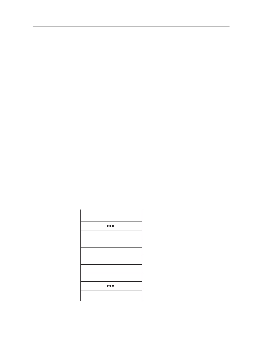
A word consists of two bytes: a high byte (bit 15 to bit 8), and a low byte
(bit 7 to bit 0) as shown in Figure 4–5. It must always align to an even address.
Figure 4–5. Byte and Word Operation
Byte1: 012h
Word1 (High Byte): 056h
xxxAh
xxx9h
xxx8h
xxx7h
xxx6h
xxx5h
xxx4h
xxx3h
Byte2: 034h
Word1 (Low Byte): 078h
Word2 (High Byte): 09Ah
Word2 (Low Byte): 0BCh
ADD.B Byte1, Byte2:
Byte2 = 012h + 034h = 046h
ADD.W Word1, Word2:
Word2 = 05678h + 09ABCh = 0F134h
All operations on the stack and PC are word operations and use even-aligned
memory addresses.