Texas Instruments MSP430x1xx User Manual
Page 414
Flash Memory Organization
C-2
C.1 Flash Memory Organization
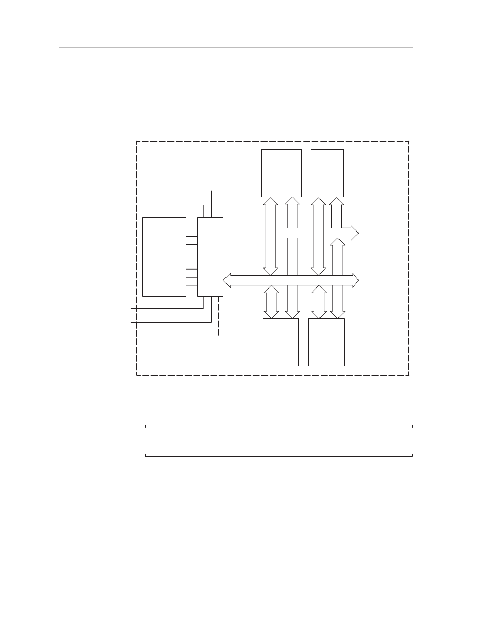
The flash memory may have one or more modules of different sizes as shown
in Figure C–1. A module is a physical memory unit that operates independent
from other modules. In an MSP430 configuration with more than one flash
memory module, all modules are located in one linear-address range.
Figure C–1.Interconnection of Flash Memory Module(s)
ROM
RAM
CPU
Incl. 16 Reg.
Test
JTAG
Flash
Memory
Module 1
MAB, 16 Bit
MDB, 16 Bit
TDI
TDO/TDI
TMS
TCK
Test/VPP
Flash
Memory
Module 2
To Other
Peripheral
Modules
Optional
Independent modules, such as Module1 and Module2, are intended to
execute software code from one module while simultaneously programming
or erasing another module.
Note:
Flash Memory Module(s) in MSP430 Devices
Different devices may have one or more flash memory modules.
If the active software and the target programming location are in the same flash
memory module, the program execution is halted (flag BUSY=1) until the pro-
gramming cycle is completed (flag BUSY=0). Then it proceeds with the next
instruction. The active software may also erase segments of the flash memory
module. The user should be careful not to erase memory locations that are
necessary to execute the software correctly.
A flash memory module, being programmed or erased, can not be accessed.
Figure C–2 shows the flash memory Module1 in program or erase operation.
During this operation the module is disconnected from the memory address