Texas Instruments MSP430x1xx User Manual
Page 434
Flash Memory Access via JTAG and Software
C-22
C.5 Flash Memory Access via JTAG and Software
C.5.1
Flash Memory Protection
Flash memory access via the serial test and programming interface JTAG can
be inhibited when the
security fuse is activated. The security fuse is activated
via serial instructions shifted into the JTAG. Activating the fuse is not revers-
ible, and any access to the internal system is disrupted. The bypass function
described in the IEEE1149.1 standard is active.
C.5.2
Program Flash Memory Module via Serial Data Link Using JTAG Feature
The hardware interconnection to the JTAG pins is done via four separate pins,
plus the ground or V
SS
reference level. The JTAG pins are TMS, TCK, TDI
(/VPP), and TDO (/TDI).
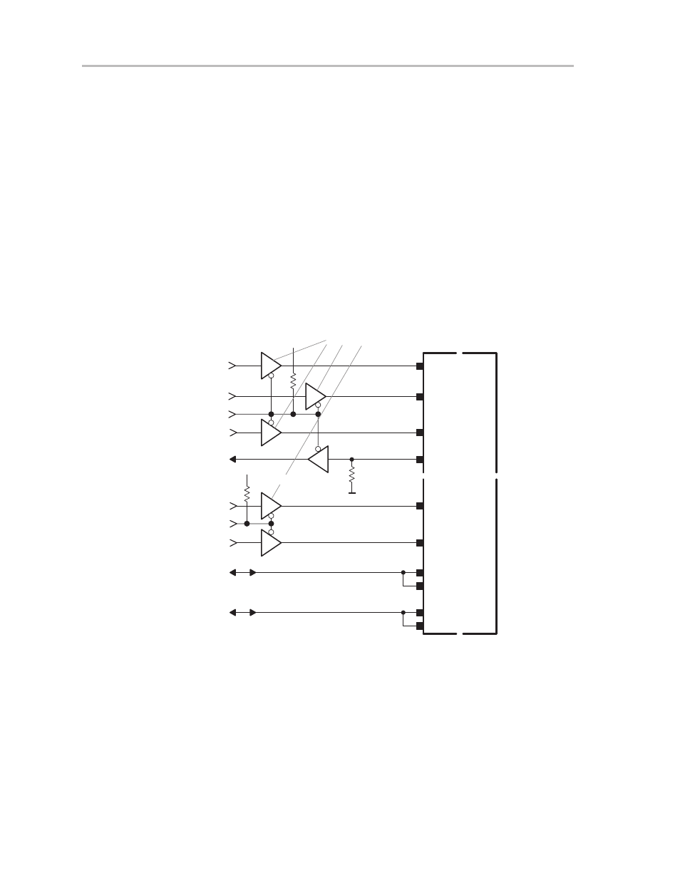
Figure C–11. Signal Connections to MSP430 JTAG Pins
TMS
TCK
TDI
TDO/TDI
MSP430Fxxx
TMS
TCK
TDI
TDO
Level Shifter
XOUT/TCLK
TCLK
EN1
68 k
Ω
TEST
Test/VPP
EN2
VCC
SN74AHC244
VCC
V
CC
/DV
CC
AV
CC
V
SS
/DV
SS
AV
SS
C.5.3
Programming a Flash Memory Module via Controller Software
No special external hardware is required to program a flash memory module.
The power supply at pin V
CC
should supply the higher current during write
(program) and erase modes. The software algorithm is simple. The embedded
timing generator in the flash memory module controls the program and erase
cycles. Software can not run in the same flash memory module where data is
to be written. Such background software needs to run on other memory
device, such as a ROM module, a RAM module, or another flash memory
module.