9 a/d grounding and noise considerations – Texas Instruments MSP430x1xx User Manual
Page 331

A/D Grounding and Noise Considerations
15-41
ADC12
15.9 A/D Grounding and Noise Considerations
As with any high-resolution converter, care and special attention must be paid
to the printed-circuit-board layout and the grounding scheme to eliminate
ground loops and any unwanted parasitic components/effects and noise.
Industry-standard grounding and layout techniques should be followed to
reduce these unwanted effects.
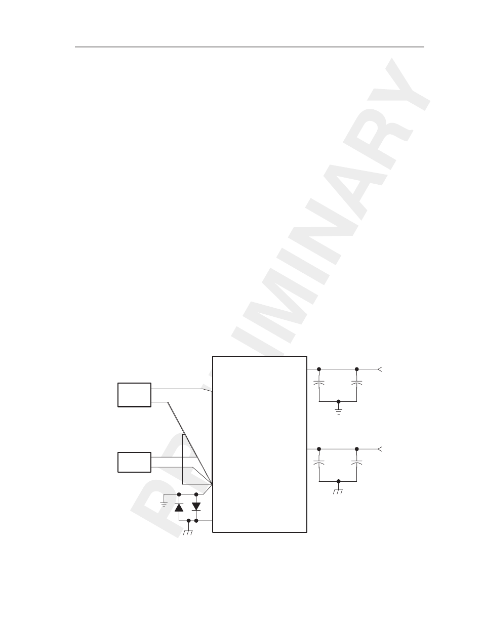
Ground Loops are formed when return current from the A/D flows through
paths that are common with other analog or digital circuitry. If care is not taken,
this current can generate small, unwanted offset voltages that can add to or
subtract from the reference or input voltages of the A/D converter. One way
to avoid ground loops is to use a star connection scheme for AV
SS
(shown in
Figure 15–26). This way the ground current or reference currents do not flow
through any common input leads, eliminating any error voltages.
The digital ground DV
SS
and analog ground AV
SS
can also be star-connected
together. If separate supplies are used, two reverse biased diodes can be used
to limit the voltage difference to less than
±
700mV.
In addition to grounding, ripple and noise spikes on the power supply lines due
to digital switching or switching power supplies can corrupt the conversion re-
sult. The ripple can become more dominant by reducing the value of the con-
version voltage range (V
R+
– V
R–
), therefore reducing the value of the LSB and
the noise margin. Thus a clean, noise-free setup becomes even more impor-
tant to achieve the desired accuracy. Adding carefully placed bypass capaci-
tors returned to the respective ground planes can help in reducing ripple in the
supply current and minimizing these effects.
Figure 15–26. A/D Grounding and Noise Considerations
ЗЗЗЗЗЗ
ЗЗЗЗЗЗ
ЗЗЗЗЗЗ
ЗЗЗЗЗЗ
ЗЗЗЗЗЗ
ЗЗЗЗЗЗ
ЗЗЗЗЗЗ
ЗЗЗЗЗЗ
ЗЗЗЗЗЗ
ЙЙЙЙЙЙ
ЙЙЙЙЙЙ
ЙЙЙЙЙЙ
22
µ
F
Tantalum
0.1
µ
F
Ceramic
AVCC
22
µ
F
Tantalum
0.1
µ
F
Ceramic
DV
CC
VREF
+
–
Ve
REF+
V
REF+
VIN
+
–
A0. . . 7
AV
SS
DV
SS
A/D
