1 introduction – Texas Instruments MSP430x1xx User Manual
Page 54

Introduction
4-2
4.1
Introduction
All of the physically separated memory areas (ROM, RAM, SFRs, and
peripheral modules) are mapped into the common address space, as shown
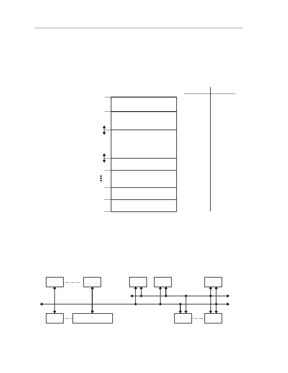
in Figure 4–1 for the MSP430 family. The addressable memory space is 64KB.
Future expansion is possible.
Figure 4–1. Memory Map of Basic Address Space
Address
(Hex.)
0FFE0h
Interrupt Vector Table
Program Memory
Branch Control Tables
Data Tables...
Data Memory
16-Bit Peripheral Modules
8-Bit Peripheral Modules
Special Function Registers
0FFFFh
0FFDFh
0200h
01FFh
0100h
0FFh
010h
0Fh
0h
Function
ROM
ROM
RAM
Timer,
ADC, . . .
I/O, LCD
8bT/C, . . .
SFR
Access
Word/Byte
Word/Byte
Word
Byte
Byte
Word/Byte
The memory data bus (MDB) is 16- or 8-bits wide. For those modules that can
be accessed with word data the width is always 16 bits. For the other modules,
the width is 8 bits, and they must be accessed using byte instructions only. The
program memory (ROM) and the data memory (RAM) can be accessed with
byte or word instructions.
Figure 4–2. Memory Data Bus
High Byte
Data Bus
SFRs
COMPARATOR_A
LCD
USART
ROM
RAM
ADC
WDT
CPU
Low Byte
Address Range 0000h – 00FFh
8-Bit Peripheral Modules,
Byte Access
Byte/Word
Access
16-Bit Peripheral Modules,
Word Access
