2 ports p1, p2, Figure 8–1. port p1, port p2 configuration – Texas Instruments MSP430x1xx User Manual
Page 123
Ports P1, P2
8-3
Digital I/O Configuration
8.2
Ports P1, P2
Each of the general-purpose ports P1 and P2 contain 8 general-purpose I/O
lines and all of the registers required to control and configure them. Each I/O
line is capable of being controlled independently. In addition, each I/O line is
capable of producing an interrupt.
Separate vectors are allocated to ports P1 and P2 modules. The pins for port
P1 (P1.0–7) source one interrupt, and the pins for port P2 (P2.0–7) source
another interrupt.
Seven registers are used to control the port I/O pins (see Section 8.2.1).
Ports P1 and P2 are connected to the processor core through the 8-bit MDB
and the MAB. They should be accessed using byte instructions in the absolute
address mode.
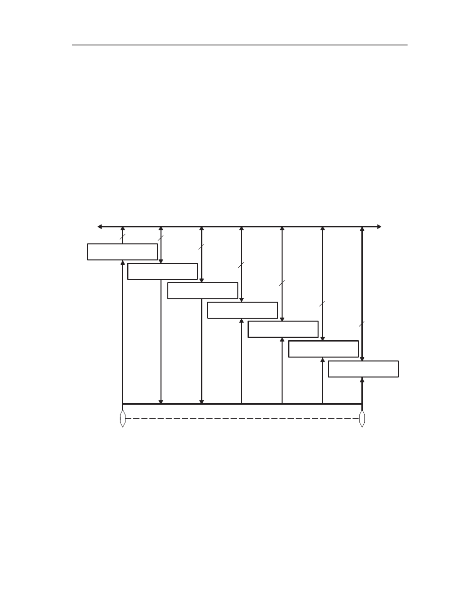
Figure 8–1. Port P1, Port P2 Configuration
Input Register PnIN
Output Register PnOUT
Direction Register
PnDIR
Interrupt Flags PnIFG
Interrupt Edge Select
PnIES
Interrupt Enable PnIE
8
8
R
R/W
8
8
R/W
R/W
8
MDB
MSB
Pn.7
LSB
Pn.0
R/W
8
R/W
n = 1: 020h
n = 2: 028h
n = 1: 021h
n = 2: 029h
n = 1: 022h
n = 2: 02Ah
n = 1: 023h
n = 2: 02Bh
n = 1: 024h
n = 2: 02Ch
n = 1: 025h
n = 2: 02Dh
Function Select PnSEL
8
R/W
n = 1: 026h
n = 2: 02Eh