5 basic clock module control registers – Texas Instruments MSP430x1xx User Manual
Page 118
Basic Clock Module Control Registers
7-18
7.5
Basic Clock Module Control Registers
The Basic Clock Module is configured using control registers DCOCTL,
BCSCTL1, and BCSCTL2, and four bits from the CPU status register: SCG1,
SCG0, OscOff, and CPUOFF. User software can modify these control
registers from their default condition at any time. The Basic Clock Module
control registers are located in the byte-wide peripheral map and should be
accessed with byte (.B) instructions.
Register
Short Form
Register Type
Address
Initial State
DCO control
register
DCOCTL
Read/write
056
h
060h
Basic clock
system control 1
BCSCTL1
Read/write
057h
084h
Basic clock
system control 1
BCSCTL2
Read/write
058h
reset
7.5.1
Digitally-Controlled Oscillator (DCO) Clock-Frequency Control
DCOCTL is loaded with a value of 060h with a valid PUC condition.
7
0
rw–0
rw–1
rw–1
rw–0
rw–0
rw–0
rw–0
rw–0
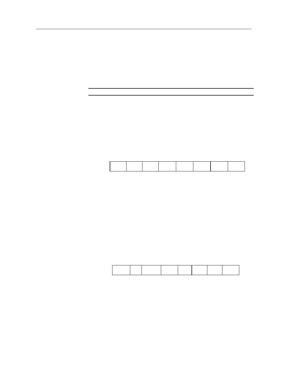
DCO.2
056h
DCOCTL
DCO.1 DCO.0 MOD.4 MOD.3 MOD.2 MOD.1 MOD.0
MOD.0 .. MOD.4:
The MOD constant defines how often the discrete
frequency f
DCO+1
is used within a period of 32 DCOCLK cycles.
During the remaining clock cycles (32–MOD) the discrete frequency
f
DCO
is used. When the DCO constant is set to seven, no modulation is
possible since the highest feasible frequency has then been selected.
DCO.0 .. DCO.2:
The DCO constant defines which one of the eight discrete
frequencies is selected. The frequency is defined by the current
injected into the dc generator.
7.5.2
Oscillator and Clock Control Register
BCSCTL1 is affected by a valid PUC or POR condition.
7
0
rw–(1)
rw–(0) rw–(0)
rw–(0) rw–0
rw–1
rw–0
rw–0
057h
BCSCTL1
XT2Off
Rsel.0
Rsel.1
Rsel.2
XTS
DIVA.1 DIVA.0 XT5V
Bit0 to Bit2:
The internal resistor is selected in eight different steps.
Rsel.0 to Rsel.2 The value of the resistor defines the nominal frequency.
The lowest nominal frequency is selected by setting Rsel=0.
Bit3, XT5V:
XT5V should always be reset.
Bit4 to Bit5:
The selected source for ACLK is divided by:
DIVA = 0: 1
DIVA = 1: 2
DIVA = 2: 4
DIVA = 3: 8