Figure 15–17. conversion timing, pulse-sample mode, And the selected sample time t – Texas Instruments MSP430x1xx User Manual
Page 315
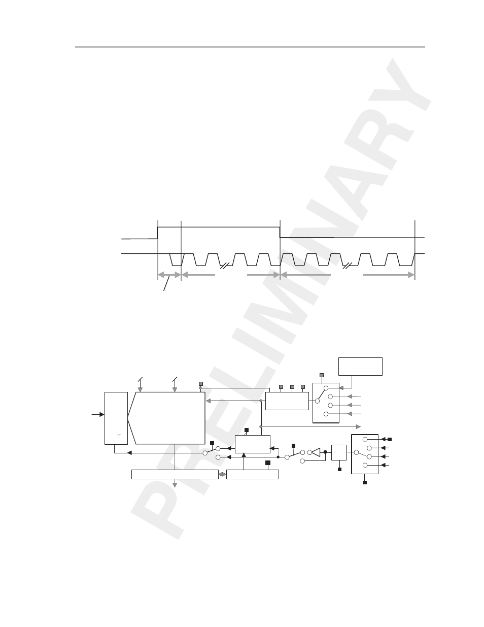
Sampling
15-25
ADC12
In pulse-sampling mode, sampling time is a multiple of the ADC12CLK x 4, and
is calculated by:
tsample = 4 x t
ADC12CLK
x SHTx
SHTx is determined by bits SHT0 or SHT1 (see table in
Control Registers
ADC12CTL0 and ADC12CTL1 section).
The sampling signal SAMPCON remains in the sampling state (high) for the
synchronization time t
sync
and the selected sample time t
sample
, as shown in
Figure 15–17. The conversion takes 13
×
ADC12CLK cycles (t
convert
). It is im-
portant to note that after a sample-and-conversion cycle has been triggered
by the sample-input signal, additional triggers (via a rising edge on the sample-
input signal) will be missed/ignored until the prior sample-and-conversion
cycle is completed.
Figure 15–17. Conversion Timing, Pulse-Sample Mode
t sync
t sample
tconvert
SAMPCON
ADC12CLK
An example of the pulse-sample mode configuration is shown in Figure 15–18.
The selected input signal source is Timer_B.OUT0. The timing for the example
is shown in Figure 15–19.
Figure 15–18. Pulse-Sample Mode Example Configuration
ACLK
MCLK
SMCLK
ADC12OSC
Internal
Oscillator
ADC12CLK
S/H
Divider by
1,2,3,4,5,6,7,8
Sampling
Timer
12–bit S A R
ADC12DIV
ISSH
SHP
SHT1
SHT0
ADC12ON
ADC12SSEL
12–bit A/D converter core
analog
input
signal
Conversion CTL
MSC
SAMPCON
SHI
SHS
ENC
ADC12SC
Timer_A.OUT1
Timer_B.OUT0
Timer_B.OUT1
SYNC
Sample
and
Hold
V
R+
V
R–