1 introduction, Adc core with sample-and-hold, Reference voltage and configuration – Texas Instruments MSP430x1xx User Manual
Page 292: Conversion clock source select and control, Sample timing and conversion control, And v, Introduction 15-2
Introduction
15-2
15.1 Introduction
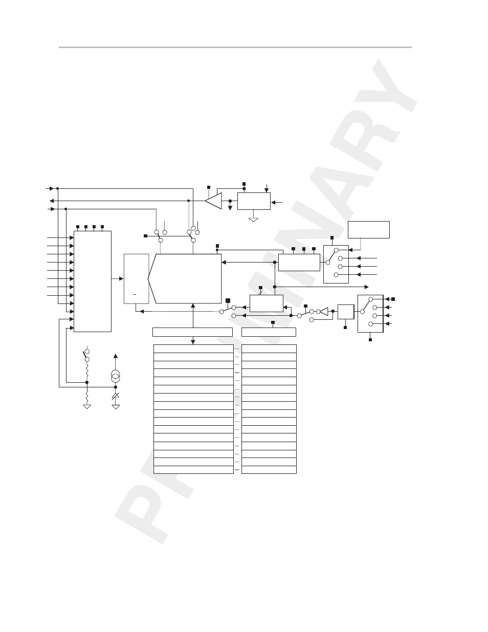
The ADC12 12-bit analog-to-digital converter (shown in Figure 15–1) has five
main functional blocks that can be individually configured and optimized:
-
ADC core with sample-and-hold
-
Conversion memory and configuration
-
Reference voltage and configuration
-
Conversion clock source select and control
-
Sample timing and conversion control
Figure 15–1. ADC12 Schematic
a0
a1
a2
a3
a4
a5
a7
a6
Analog
Multiplexer
12 : 1
1.5V or 2.5V
V
REF+
Sample
Hold
ACLK
MCLK
SMCLK
ADC12OSC
Internal
Oscillator
ADC12CLK
S/H
Divide by
1,2,3,4,5,6,7,8
Sampling
Timer
a8
a9
a10
a11
12–bit S A R
ADC12DIV
REFON
2_5V
ISSH
SHP
ADC12CTLx.0..3
ADC12CTLx.4..6
T
SHT1
SHT0
ADC12ON
ADC12SSEL
VeREF
+
V
REF+
V
REF–
/
VeREF–
V
R+
V
R–
12–bit A/D converter core
Conversion CTL
MSC
Ref_X
INCH= 0Ah
Ref_X
SAMPCON
Reference
on
on
0140h
0142h
015Ch
015Eh
080h
081h
08Eh
08Fh
ADC12MEM0
ADC12MEM1
ADC12MEM14
ADC12MEM15
16 x 12–bit
ADC Memory
16 x 8–bit
ADC Memory Control
ADC12MEM10
ADC12MEM9
ADC12MEM8
ADC12MEM6
ADC12MEM7
ADC12MEM5
ADC12MEM11
ADC12MEM4
ADC12MEM3
ADC12MEM2
ADC12MEM12
ADC12MEM13
ADC12CTL0
ADC12CTL1
ADC12CTL2
ADC12CTL3
ADC12CTL4
ADC12CTL5
ADC12CTL6
ADC12CTL7
ADC12CTL8
ADC12CTL9
ADC12CTL10
ADC12CTL11
ADC12CTL12
ADC12CTL13
ADC12CTL14
ADC12CTL15
082h
083h
084h
085h
086h
088h
087h
089h
08Ah
08Bh
08Ch
08Dh
0144h
0146h
0148h
014Ah
014Ch
014Eh
0150h
0152h
0154h
0156h
0158h
015Ah
SHI
SHS
ENC
ADC12SC
Timer_A.OUT1
Timer_B.OUT0
Timer_B.OUT1
SYNC
AVSS
AVCC
AVSS
AVSS
AVCC
and
AVCC
The ADC12 can convert one of eight external analog inputs, or one of four
internal voltages. The four internal channels are used for temperature
measurement (via on-chip temperature diode), and for measurement of Vcc
(via Vcc/2) and the positive and negative references applied on Ve
REF+
and
V
REF–
/Ve
REF–
.
The ADC12 can use its internal reference, or it can use external reference(s)
or a combination of internal and external reference-voltage levels.