2 adc12 description and operation, 1 adc core – Texas Instruments MSP430x1xx User Manual
Page 294

ADC12 Description and Operation
15-4
-
Versatile conversion modes including single-channel, repeated single-
channel, sequence, and repeated sequence.
-
Sixteen 12-bit registers for storage of conversion results. Each register is
individually accessible by software and individually configurable to define
the channel and references for its conversion result.
-
ADC core and reference voltage powered down separately
15.2 ADC12 Description and Operation
15.2.1 ADC Core
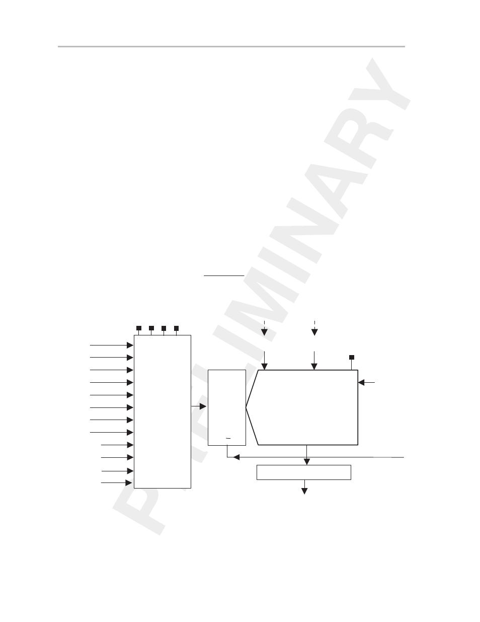
The ADC core (shown in Figure 15–2) converts the analog input to its 12-bit
representation and stores the results in the conversion memory. The core uses
two programmable/selectable voltage levels (V
R+
and V
R–
) to define the upper
and lower limits of the conversion range, and to define the full-scale and
zero-scale readings. The digital output is full scale when the input signal is
equal to or higher than V
R+
, and zero when the input signal is equal to or lower
than V
R–
. The input channel and the reference voltage levels (V
R+
and V
R–
)
are defined in the conversion-control memory. The conversion formula is:
N
ADC
+
4095
Vin – V
R–
V
R
)
– V
R–
Figure 15–2. ADC Core, Input Multiplexer, and Sample-and-Hold
a0
a1
a2
a3
a4
a5
a7
a6
Analog
Multiplexer
12 : 1
Sample
and
Hold
ADC12CLK
S/H
a8
a9
a10
a11
ADC12MCTLx.0..3
12–bit A/D converter core
SAMPCON
ADC12ON
from Reference
S A R
to ADC12MEMx
Temperature
ADC12MCTLx.4..6
VR–
VR+
VeREF+
VeREF–/
VREF–
AVCC/2
It is important to note that the 3 LSBs of the conversion are resolved resistively.
Therefore, when the 3 LSBs are being resolved during a conversion, approxi-
mately 200
µ
A will be required from the reference. The user should keep this
in mind when choosing and decoupling an external reference. Refer to the de-
vice data sheet for more details on ADC12 specifications.
