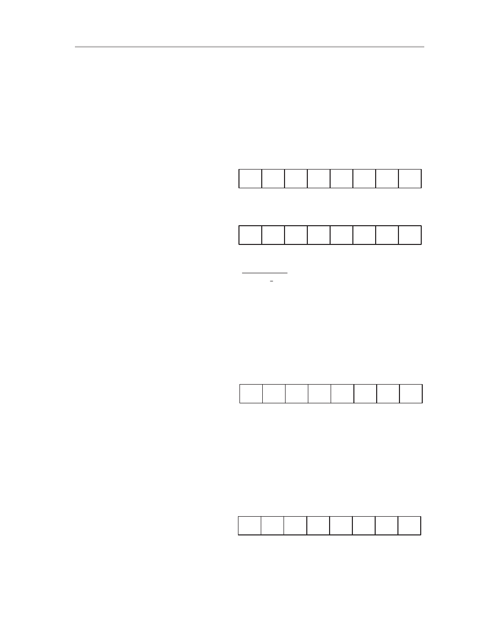
Figure 13–19. usart baud-rate select register, Figure 13–20. usart modulation control register, 5 receive data buffer urxbuf – Texas Instruments MSP430x1xx User Manual
Page 265: Figure 13–21. receive data buffer urxbuf

Control and Status Registers
13-19
USART Peripheral Interface, SPI Mode
transition signal to pin STE. FE is reset by a SWRST, a system
reset, by reading the URXBUF, or by an instruction.
13.5.4 Baud-Rate Select and Modulation Control Registers
The baud-rate generator uses the content of baud-rate select registers UBR1
and UBR0, shown in Figure 13–19, to generate the serial-data-stream bit
timing. The smallest division factor is two.
Figure 13–19. USART Baud-Rate Select Register
27
7
0
UBR00, 074h
26
25
24
23
22
21
20
rw
215
7
0
UBR10, 075h
214
213
212
211
210
29
28
rw
rw
rw
rw
rw
rw
rw
rw
rw
rw
rw
rw
rw
rw
rw
UBR01, 07Ch
UBR11, 07Dh
Baud rate =
BRCLK
UBR
)
1
n
S
n
i
mi
with UBR= [UBR1,UBR0]
The maximum baud rate that can be selected for transmission in master mode
is half of the clock-input frequency of the baud-rate generator. In slave mode,
the rate is determined by the external clock applied to UCLK.
The modulation control register, shown in Figure 13–20, is not used for serial
synchronous communication. It is best kept in reset mode (bits m0 to m7 = 0).
Figure 13–20. USART Modulation Control Register
7
0
UMCTL0, 073h
m3
m7
m6
m5
m2
m4
m1
m0
rw
rw
rw
rw
rw
rw
rw
rw
UMCTL1, 07Bh
13.5.5 Receive Data Buffer URXBUF
The receive data buffer (URXBUF), shown in Figure 13–21, contains previous
data from the receiver shift register. URXBUF is cleared with a SWRST or a
PUC signal. Reading URXBUF resets the receive-error bits and the receive-
interrupt flag URXIFG.
Figure 13–21. Receive Data Buffer URXBUF
27
7
0
URXBUF0, 076h
26
25
24
23
22
21
20
rw
rw
rw
rw
rw
rw
rw
rw
URXBUF1, 07Eh
The MSB of the URXBUF is always reset in seven-bit-length mode.
